
Battle for High-Density Assembly: How to Multidimensionally Evaluate and Compare BGA PCB Suppliers’ Real Strength?
In modern electronic product development, BGA chips are increasingly widely used. Many engineering teams feel extremely stressed when selecting partner factories. People frequently face potential hazards like open solder joints and cold solder joints. Therefore, choosing an experienced printed circuit board manufacturer can significantly reduce costly rework risks. You can gain a deep understanding of professional evaluation systems through this article.

1. Manufacturing Capabilities and Process Precision Comparison: Intercepting Fine Pitch Packaging Hard Strength
Evaluating suppliers first requires examining the factory’s actual processing limits for micro pads.
1.1 0.4mm and Below Pitch Pad Tolerances and VIPPO Plating Plug Capability
High-precision line width and spacing play a decisive role in pad forming. Excellent factories can precisely master via-in-pad resin plugging processes. Furthermore, technicians strictly control solder mask opening tolerances within micron levels. Precise alignment tolerances effectively prevent short-circuit bridging between pads.
1.2 Multilayer Board Lamination Warpage Control and CTE Matching
High-multilayer circuit boards easily deform when facing reflow soldering temperatures. Factories must adopt symmetrical stackup structures and pre-baking stress relief workflows. As a result, thermal pressure warpage is strictly limited within a minimal range. Flat board surfaces guarantee proper contact between chip solder balls and pads.

2. Quality Control and Inspection Matrix Comparison: Nondestructive Interception Net from X-Ray to AOI
BGA solder joints are hidden beneath chips, making visual inspection impossible for quality determination.
2.1 3D X-Ray Tomography Scanning and BGA Voiding Rate Control
Contract manufacturers must be equipped with high-resolution 3D X-Ray inspection instruments. Quality inspectors can perform perspective spot checks on every hidden solder joint. Thus, technical teams control solder ball voiding rates to extremely low ratios according to IPC standards. Strict metrics eliminate high-frequency signal attenuation caused by air pockets.
2.2 Automated Optical Inspection and Flying Probe/Bed-of-Nails Electrical Testing
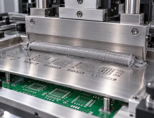
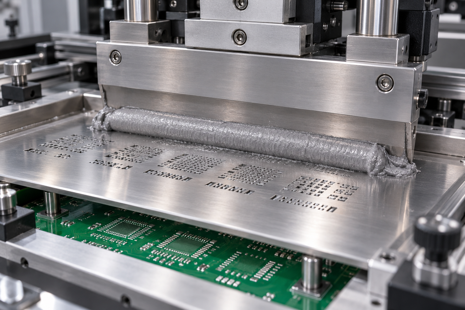
Production lines use 3D solder paste inspection before component placement to intercept printing defects. Optical inspection equipment precisely captures component shifts and tombstoning after placement. At the same time, circuit functional testing thoroughly verifies electrical continuity among dense pins. Comprehensive inspection processes ensure first-pass yield for finished products.

3. Delivery Timeliness and Supply Chain Resilience Comparison: Balancing Quick Prototyping and Mass Production
Delivery speed depends on placement efficiency, and it also depends on early engineering collaboration capabilities.
3.1 Rapid DFM Engineering Review Response Mechanism
Professional factories feature efficient engineering pre-review teams. Technicians can rapidly conduct in-depth analysis on design files and bills of materials. So, teams can identify pad defects and thermal dissipation issues early. Early reviews eliminate production interruptions and repeated revision risks.
3.2 Quick-Turn Prototyping and Flexible Small-to-Medium Batch Scheduling
Qualified suppliers need dedicated quick-turn production lines. Factories can rapidly complete complex board prototyping within a few days. In addition, strong supply chain flexibility guarantees material supply during urgent changes. Flexible scheduling mechanisms fulfill customers’ tight delivery demands.
4. Overall Cost and Hidden Expense Analysis: Economic Accounts Beyond the Quotation Sheet
Procurement teams cannot look solely at surface quotes; they need to calculate full-lifecycle comprehensive costs.

4.1 Material Degradation and Inspection Cutbacks Behind Low-Price Quotes
Low-cost contract factories often use inferior base materials with low heat resistance. Some factories even skip expensive X-Ray spot check procedures. Consequently, hidden cold solder defects cause field maintenance costs to skyrocket later. Inferior materials ultimately force buyers to pay a heavy price.
4.2 Achieving Genuine Cost Reduction Through Transparent Professional Manufacturing
Choosing our professional smart manufacturing services solves high chip scrap rate pain points. Choosing our transparent factory services solves high overseas engineering communication cost challenges. Now, you can guarantee smooth project progression through full-process transparent management.
5. Conclusion and BGA Engineering Evaluation Channel
Evaluating qualified suppliers requires comprehensive consideration of processing capabilities and inspection methods.
Now, you can directly submit Gerber files to the online evaluation platform. Authoritative printed circuit board manufacturer teams will provide free professional evaluation reports for you. Transparent cost-effective solutions will help your electronic products reach the market quickly.










Leave A Comment