
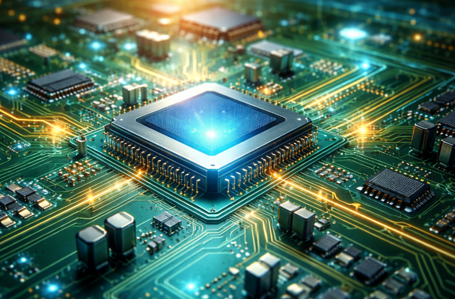
From Bare Board to Smart Devices: A Deep Dive into the Full PCB & PCBA Manufacturing Process
In the electronics manufacturing industry, PCB and PCBA are the backbone of every product lifecycle. From a simple copper-clad laminate to a complex intelligent device, the journey involves interdisciplinary expertise across materials science, electronic engineering, and precision manufacturing. This article provides a systematic breakdown of key PCB and PCBA technologies, processes, and industry trends to help build a comprehensive understanding.
1. PCB Fundamentals: The “Neural Network” of Electronics
A PCB (Printed Circuit Board) serves as both the physical support and electrical interconnection platform for electronic components. Based on structure, PCBs are categorized into single-sided, double-sided, multilayer boards, and HDI (High Density Interconnect) boards.
In high-end applications, multilayer boards increase routing density and reduce electromagnetic interference (EMI). HDI boards further enhance integration through technologies such as microvias and buried vias.
1.1 Core Materials
PCB performance heavily depends on its material system:
- Substrate: Commonly FR-4 (glass fiber-reinforced epoxy)
- Copper foil: Determines conductivity and signal performance
- Copper thickness: Typically measured in ounces (oz)
For high-speed designs, dielectric constant (Dk) and dissipation factor (Df) are critical, directly impacting signal integrity (SI) and power integrity (PI).
 2. PCB Manufacturing Process Explained
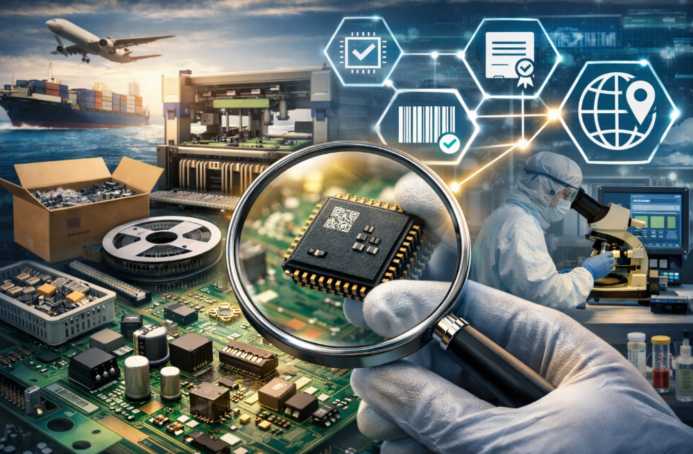
PCB fabrication is a complex process chain that includes the following key steps:
2.1 Inner Layer Processing
Photoplotting is used to generate circuit patterns, followed by exposure and development to form the circuitry.
2.2 Lamination
Multilayer boards are formed by pressing inner layers with prepreg under high temperature and pressure.
2.3 Drilling and Plating
- Mechanical drilling
- Laser drilling
This is followed by via metallization (plating) to ensure electrical connectivity.
2.4 Outer Layer Formation and Surface Finish
Common surface finishes include:
- HASL (Hot Air Solder Leveling)
- ENIG (Electroless Nickel Immersion Gold)
- OSP (Organic Solderability Preservative)
Each option involves trade-offs in solderability, flatness, and cost.
 3. PCBA: From “Board” to “System”
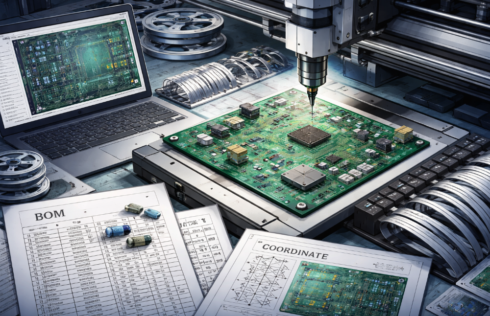
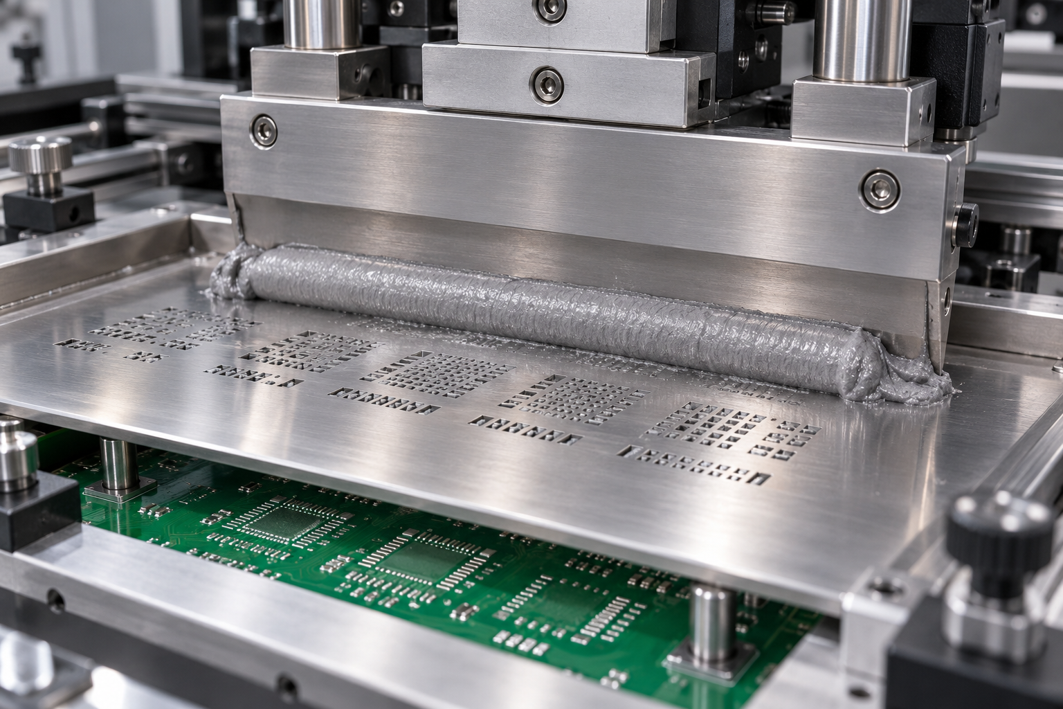
PCBA (Printed Circuit Board Assembly) refers to the process of assembling electronic components onto the PCB, transforming it into a functional system.
3.1 SMT and THT Technologies
SMT (Surface Mount Technology)
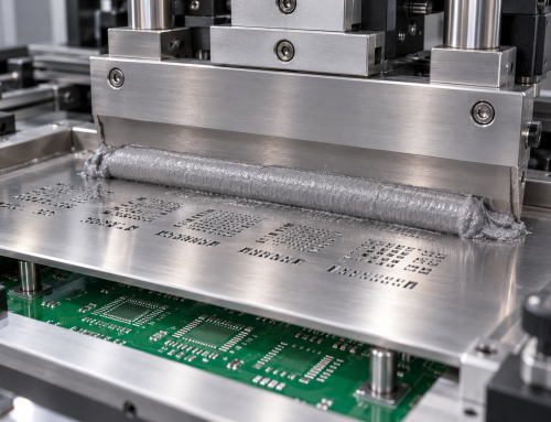
- Components are placed using pick-and-place machines
- Reflow soldering completes the bonding process
THT (Through-Hole Technology)
- Components are inserted and soldered via wave soldering
Modern electronics primarily rely on SMT, while THT remains essential in high-reliability applications.
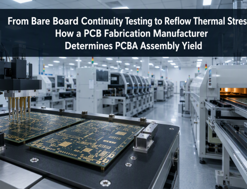
3.2 Soldering Quality Control
Solder joint quality directly impacts product reliability. Common defects include:
- Cold joints
- Solder bridging
- Voiding
Inspection methods include:
- AOI (Automated Optical Inspection)
- X-ray inspection
- ICT (In-Circuit Testing)
4. Design Essentials: DFM and DFT
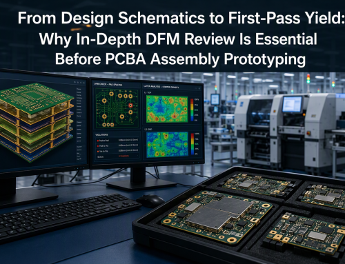
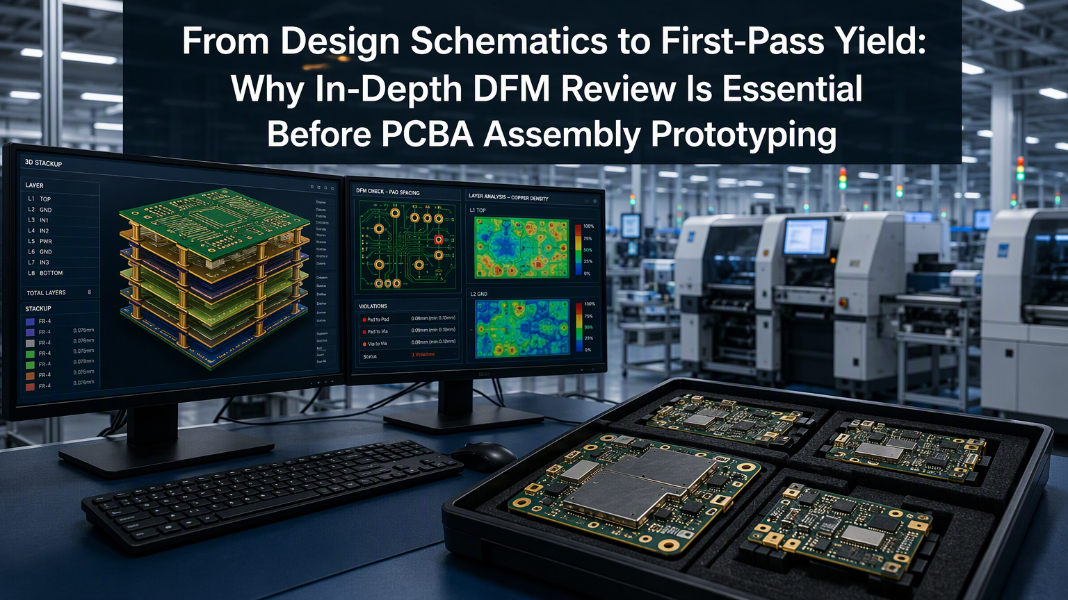
In PCB/PCBA development, DFM (Design for Manufacturability) and DFT (Design for Testability) are crucial for improving yield and reducing costs.
4.1 DFM Guidelines
- Proper pad design
- Optimized trace spacing
- Impedance control
4.2 DFT Strategies
- Add test points
- Implement boundary scan
- Increase test coverage
 5. High-Speed and High-Frequency Design Challenges
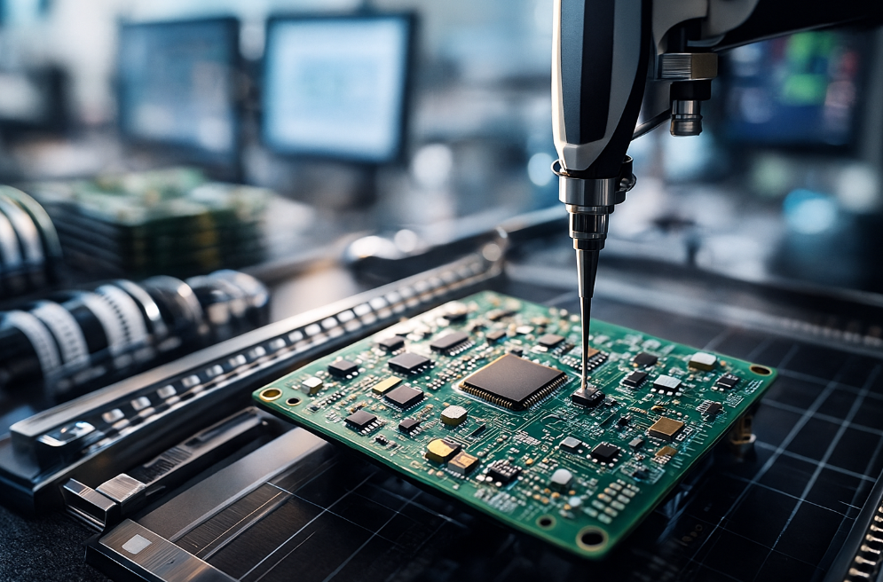
With the rise of 5G, AI, and IoT, PCB design is entering a high-speed, high-frequency era. Key challenges include:
- Signal integrity (SI) issues
- Crosstalk
- Timing skew
Solutions include differential pair routing, impedance control, and optimized stack-up design.
6. Industry Trends: Toward High Density and Smart Manufacturing
6.1 HDI and IC Substrates
With advancements in semiconductor packaging, IC substrates have become a critical segment of high-end PCBs.
6.2 Automation and Smart Manufacturing
- Smart factories
- MES (Manufacturing Execution Systems)
- Data-driven process optimization
6.3 Green Manufacturing
Environmental regulations are driving the adoption of lead-free processes and energy-efficient manufacturing technologies.
PCB and PCBA are not only the foundation of electronic products but also key drivers of technological innovation. From material selection to manufacturing processes and design optimization, every step affects performance and reliability.
Looking ahead, the PCB industry will continue evolving toward higher precision, reliability, and integration. Companies that master core processes, optimize design workflows, and embrace digital transformation will gain a significant competitive advantage.

Leave A Comment