

From Chaos to Efficiency: Advanced Auto‑Routing Techniques for Modern PCB Design
1. The Role of Auto Routing in Modern PCB Design
In modern electronic product development, PCB design efficiency directly affects the product’s time‑to‑market. With the rapid growth of high‑speed and high‑density circuits, engineers are facing increasingly complex routing challenges. As a result, auto routing has become an important function in many PCB design tools.
Auto routing is not simply about letting software replace engineers. Instead, it represents a design methodology that combines rule‑driven design with engineering experience. When used correctly, auto routing can significantly improve design efficiency while still maintaining strong signal integrity.
However, without the correct strategy, auto routing may introduce problems such as crosstalk, impedance discontinuity, and incomplete return paths. Therefore, understanding the logic behind auto‑routing engines is essential for achieving high‑quality PCB designs.
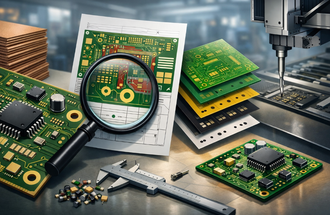 2. Essential Preparation Before Auto Routing
2.1 Accurate Design Rule Configuration
The quality of auto routing is largely determined by the completeness of the design rules. Common parameters that must be defined before routing include:
- Trace width
- Trace clearance
- Differential pair spacing
- Controlled impedance rules
- Via types and sizes
By establishing a clear rule set in the EDA environment, the auto‑routing engine can complete routing tasks while meeting manufacturing requirements and design for manufacturability (DFM) standards.
2.2 Proper Component Placement
There is a well‑known saying in PCB design:
Placement determines 70% of routing quality.
Auto‑routing tools cannot compensate for poor component placement. If critical chips are placed too far apart or interface directions are disorganized, the routing process will generate unnecessary detours and excessive vias.
Effective component placement should follow several principles:
- Arrange components according to signal flow
- Place high‑speed devices close to connectors
- Separate analog and digital regions
- Concentrate power management components
2.3 Early Planning of Power and Ground Planes
Auto‑routing tools typically have limited capability when dealing with power networks. Therefore, designers should plan power and ground layers in advance.
Common best practices include:
- Using a solid ground plane
- Separating power domains
- Placing decoupling capacitors close to high‑frequency power pins
These practices help maintain continuous return paths and reduce noise issues in high‑speed circuits.
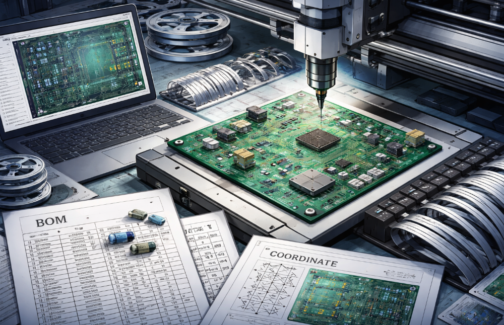 3. Key Techniques to Improve Auto Routing Efficiency
3.1 Manually Route Critical Nets First
Certain signal types should not rely entirely on auto routing, including:
- High‑speed differential signals (USB, PCIe, etc.)
- Clock signals
- RF transmission lines
- Length‑matched buses
Engineers should manually route these critical nets first and then allow the auto router to handle standard signal connections.
3.2 Use Region‑Based Routing Strategies
Many modern EDA tools support room‑based or region‑based routing. Designers can divide the PCB into functional areas such as power sections, processor areas, and interface zones.
This method prevents the auto router from crossing multiple functional blocks unnecessarily, improving routing clarity and reducing long trace paths.
3.3 Optimize Via Usage
Auto routers tend to generate a large number of vias. Without proper constraints, this can cause several issues:
- Reduced signal integrity
- Increased manufacturing cost
- Higher electromagnetic interference (EMI)
Designers can optimize routing results by limiting via counts or specifying preferred via structures.
3.4 Combine Push‑and‑Shove Routing Technology
Modern PCB design tools often include push‑and‑shove routing capabilities. When a new trace enters a congested area, the system automatically shifts nearby traces while maintaining design rule compliance.
This technique allows higher routing density while ensuring that electrical constraints remain satisfied.
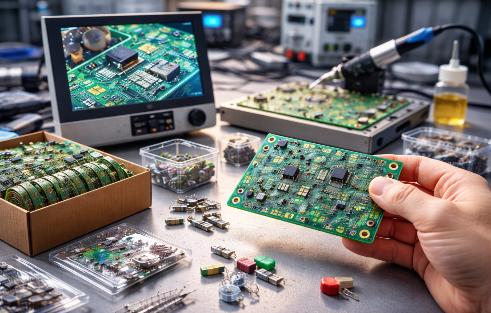 4. Post‑Routing Optimization and Verification
4.1 Signal Integrity Analysis
After auto routing is completed, signal integrity (SI) analysis should be performed to evaluate:
- Impedance continuity
- Signal reflections
- Crosstalk
- Propagation delay
If necessary, critical traces should be manually adjusted to meet performance requirements.
4.2 Design for Manufacturability (DFM) Checks
Automatically generated routing may introduce manufacturing issues such as:
- Insufficient trace spacing
- Small annular rings around vias
- Isolated copper areas
Performing DFM checks helps identify potential production risks before fabrication begins.
4.3 Improving Routing Cleanliness
Although electrical performance comes first, visually clean routing can improve engineering readability and maintenance.
Typical optimization steps include:
- Reducing unnecessary trace bends
- Maintaining consistent routing angles
- Removing redundant vias
A well‑organized PCB layout often reflects a more stable and reliable electrical design.
5. The Future of Auto Routing Technology
With the development of artificial intelligence and advanced EDA algorithms, auto routing is entering a new stage of evolution. Some advanced PCB design platforms are beginning to integrate machine learning to optimize routing strategies based on historical design data.
Future auto‑routing systems may offer capabilities such as:
- Automatic identification of critical nets
- Real‑time signal integrity evaluation
- Intelligent placement recommendations
- Automated power integrity optimization
For PCB engineers, auto routing will not replace engineering expertise, but it will continue to serve as a powerful tool for improving productivity.
Auto routing has become an essential tool in modern PCB design. However, excellent PCB layouts still rely heavily on engineering knowledge and strategic decision‑making. By carefully defining design rules, optimizing component placement, and performing post‑routing verification, designers can maximize the benefits of auto routing.
As electronic systems continue to become faster and more complex, mastering auto‑routing techniques will be a critical skill for PCB engineers seeking to improve both design efficiency and product reliability.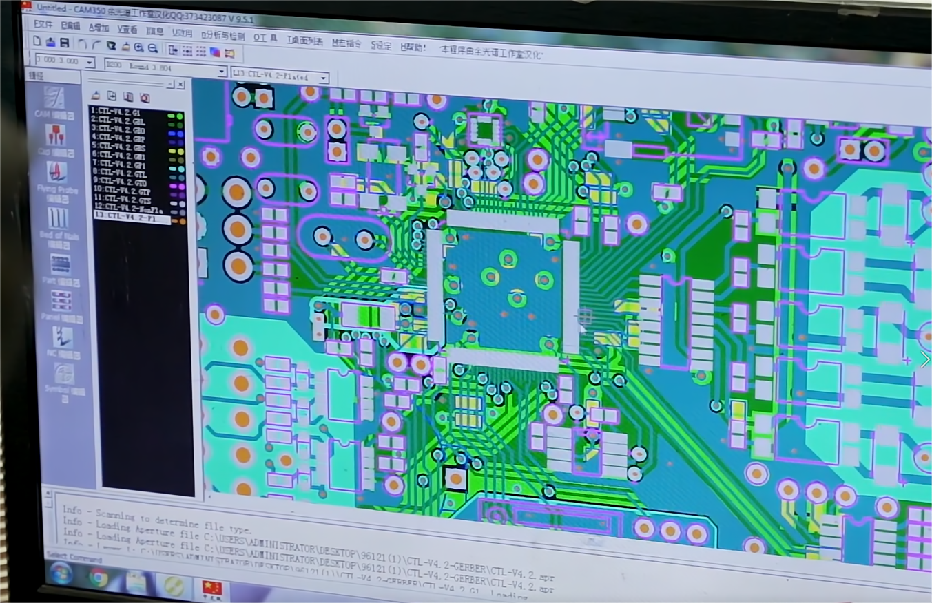







Leave A Comment