

From Prototype Validation to Advanced Manufacturing: Where Is PCB Printing Truly Applied?
As the electronics manufacturing industry continues to evolve toward higher density, miniaturization, and enhanced reliability, PCB printing technology has gradually shifted from being a supporting process to a core manufacturing discipline. Whether in product prototyping, low-volume production, or specialized electronic applications, PCB Printing plays an irreplaceable role.
This article focuses on the key question: “What scenarios is PCB Printing mainly suitable for?” We will explore three major dimensions—prototype development, low-volume manufacturing, and specialized applications—while integrating professional concepts such as Surface Mount Technology (SMT), stencil printing, solder paste deposition, fine-pitch assembly, and process control strategies. The goal is to provide a comprehensive and technically grounded understanding of its practical boundaries and advantages.
 1. What Is PCB Printing? Understanding Its Process Fundamentals
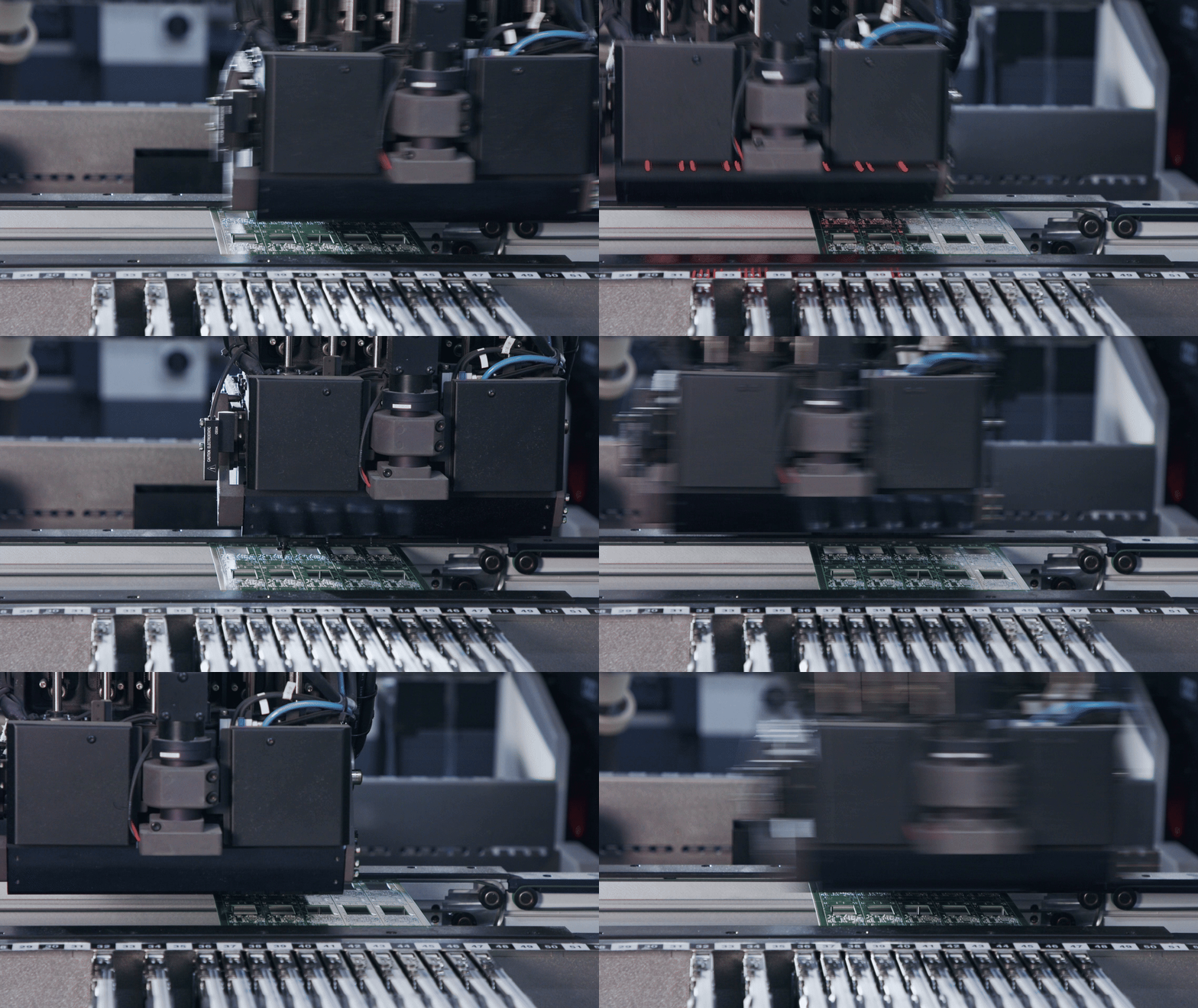 1. What Is PCB Printing? Understanding Its Process Fundamentals
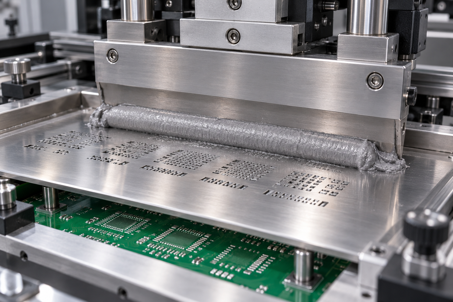
PCB Printing generally refers to the process of accurately depositing solder paste, conductive ink, or insulating materials onto designated areas of a Printed Circuit Board (PCB) using a stencil or screen.
Within the PCBA (Printed Circuit Board Assembly) workflow, solder paste printing quality directly affects downstream processes such as pick-and-place assembly, reflow soldering, and Automated Optical Inspection (AOI). Critical parameters typically include:
- Stencil thickness control
- Paste release ratio
- Alignment accuracy
- Solder Paste Inspection (SPI) data analysis
Because these variables significantly influence assembly reliability, the role of PCB Printing varies depending on the production stage.
2. Prototype Stage: A Critical Tool for Rapid Design Validation
2.1 Why Prototype Development Relies Heavily on PCB Printing
During the early product development phase, engineers often conduct multiple rounds of design verification. At this stage, priorities include:
- Quick-turn PCB fabrication
- Flexible design modification
- Controlled trial production cost
PCB Printing provides distinct advantages in prototype development.
(1) Supporting Small Quantities with Frequent Iterations
Prototype builds typically range from 5 to 50 pieces, but design revisions occur frequently. By using laser-cut stencils or reusable framed stencil systems, solder paste preparation can be completed quickly, shortening the New Product Introduction (NPI) cycle.
(2) Enabling Fine-Pitch and High-Density Package Validation
When validating BGA, QFN, or 0.4 mm pitch IC packages, solder paste deposition accuracy determines the risk of solder bridging or cold joints. High-precision printing equipment combined with SPI systems allows early detection of manufacturability issues.
(3) Controlling Costs While Encouraging Iterative Testing
Compared with tooling-intensive processes, PCB Printing requires relatively low upfront investment, making it suitable for multiple design verification cycles without excessive financial burden.
Summary
In the prototype phase, PCB Printing emphasizes flexibility and precision rather than maximum throughput. It plays a vital role in validating pad design, solder mask openings, and overall Design for Manufacturability (DFM).
3. Low-Volume Production: Balancing Cost and Consistency
 3. Low-Volume Production: Balancing Cost and Consistency
3.1 Characteristics of Low-Volume PCBA Manufacturing
Low-volume production typically refers to orders ranging from 100 to 5,000 units. It is common in:
- Industrial control equipment
- Medical electronics
- Communication modules
- Customized electronic terminals
At this stage, manufacturers must maintain stable quality while controlling total BOM costs.
3.2 Advantages of PCB Printing in Low-Volume Manufacturing
(1) Improving Yield and Reducing Rework
Stable solder paste volume control significantly reduces rework rates. By optimizing stencil aperture design and applying nano-coated stencil technology, manufacturers can improve paste release performance and printing consistency.
(2) Supporting Mixed Assembly Processes (SMT + THT)
Many low-volume projects use a combination of SMT and Through-Hole Technology (THT). PCB Printing demonstrates flexibility through selective printing strategies and step stencil applications.
(3) Enabling High-Mix, Low-Volume Manufacturing
In multi-product production environments, printing equipment can quickly switch programs and adjust parameters, enabling flexible manufacturing while maintaining process stability.
Summary
For low-volume PCBA manufacturing, PCB Printing focuses on consistency and repeatability. It is a core process that supports high yield rates and traceability control.
4. Specialized Applications: A Gateway to Advanced and Functional Electronics
Beyond prototyping and low-volume production, PCB Printing also plays a critical role in advanced technical applications.
4.1 High-Density Interconnect (HDI) and Microelectronics
In HDI boards featuring microvias and ultra-fine trace designs, solder paste deposition windows are extremely small. Printing accuracy may need to reach ±12.5 μm. Such applications demand:
- Electropolished stencils
- Ultra-thin stencils (≤80 μm)
- Vacuum printing systems
4.2 Power Electronics and Heavy Copper PCBs
In electric vehicle systems and power modules, heavy copper PCBs and large current pads often create uneven solder paste distribution. Zonal printing strategies and multiple-pass printing techniques can help optimize thermal balance.
4.3 Flexible Circuits and Rigid-Flex Boards
Flexible Printed Circuits (FPC) and rigid-flex PCBs require careful control of printing pressure and customized support fixtures. Low-pressure printing parameters are critical to avoid deformation and ensure deposition accuracy.
4.4 Conductive Ink and Functional Printing
In wearable devices and sensor circuits, PCB Printing extends beyond solder paste to include silver paste, carbon ink, and other functional materials. These materials are used to form antennas, electrodes, or heating elements, transforming printing from a purely assembly process into a functional enabling technology.
Summary
In specialized applications, PCB Printing is not merely an assembly-supporting process; it becomes a platform for technological innovation and functional realization.
5. Prototype, Low Volume, or Specialized Application: How to Choose
The focus of PCB Printing shifts significantly depending on the application scenario.
In the prototype stage, the primary objective is design validation. Precision, parameter flexibility, and rapid engineering support are the main priorities. Efficiency is secondary to adaptability.
In low-volume production, the goal shifts to stable yield performance and cost management. Printing consistency, solder paste volume control, and SPI data loop management become essential. Production rhythm and traceability also play important roles.
In specialized applications such as HDI, power electronics, or functional material printing, the objective becomes technological breakthrough and process innovation. These scenarios often require customized stencil design, advanced material handling, and high-end equipment support, demanding strong process development capabilities.
6. The Real Value of PCB Printing
PCB Printing is not limited to a single production stage. It acts as an accelerator for prototype validation, a stabilizer for low-volume manufacturing, and a technological enabler for advanced electronic production.
As electronic products continue to move toward smaller form factors, higher frequencies, and greater power densities, solder paste deposition accuracy, printing repeatability, and data-driven monitoring capabilities will become decisive factors in overall PCBA quality.
For electronics engineers and procurement decision-makers, understanding the practical application scenarios and technical boundaries of PCB Printing is essential for optimizing supply chains and improving product reliability.

Leave A Comment