
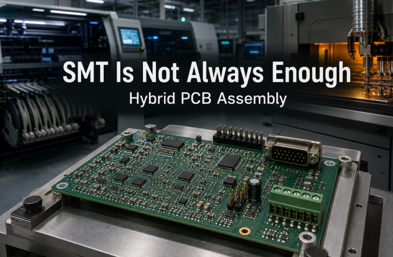
SMT Is Not Always Enough: How Hybrid PCB Assembly Is Solving Modern PCBA Challenges
Modern electronics are becoming smaller, smarter, and more densely integrated. Surface-mount technology has become the dominant method for assembling electronic components, allowing manufacturers to place thousands of components onto compact PCB layouts.
But there is a misconception in modern PCBA manufacturing:
If SMT can handle high-density assembly, why do manufacturers still need through-hole components?
The answer lies in the fact that not every electronic component, mechanical requirement, or electrical application can be optimized through SMT alone.
Connectors, transformers, high-power components, switches, relays, large capacitors, and mechanically stressed components may still require Through-Hole Technology (THT).
This has created a manufacturing approach that combines two different assembly technologies on the same PCB:
SMT + THT = Hybrid PCB Assembly
Hybrid assembly is not simply a compromise between old and new manufacturing methods. It is a deliberate engineering strategy that combines the density and automation of SMT with the mechanical strength and flexibility of through-hole assembly.
For many industrial, automotive, communication, power electronics, and control applications, this combination can determine whether a PCBA is practical to manufacture.
 What Is Hybrid PCB Assembly?
Hybrid PCB assembly refers to a manufacturing process in which a single PCB contains both surface-mount components and through-hole components.
SMT components are mounted directly onto copper pads on the PCB surface.
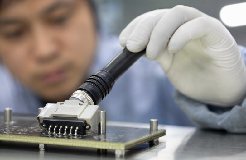
THT components, in contrast, use leads that pass through drilled holes in the PCB and are soldered to corresponding pads.
A typical hybrid PCBA may contain:
- 0201 or 0402 passive components
- QFN or QFP packages
- BGA devices
- Through-hole connectors
- Large capacitors
- Relays
- Transformers
- Power inductors
- Terminal blocks
- Mechanical switches
This combination allows engineers to choose the most appropriate package and mounting method for each component instead of forcing the entire PCB to follow a single assembly technology.
Why Are Through-Hole Components Still Relevant?
SMT provides excellent component density and manufacturing efficiency, but mechanical strength is one area where THT can offer significant advantages.
Consider a PCB containing a large connector.
Every time a user inserts or removes a cable, mechanical force is transferred into the connector.
If the connector is mounted only on the PCB surface, the solder joints must absorb a substantial portion of that mechanical stress.
A through-hole connector transfers part of the mechanical load through the component leads and PCB structure.
This makes THT particularly useful for components exposed to:
- Repeated insertion
- Mechanical vibration
- Cable movement
- Shock
- High mechanical loads
This is one reason connectors and other mechanically demanding components continue to appear in modern PCB designs.
 SMT and THT Solve Different Problems
The real advantage of hybrid assembly comes from understanding that SMT and THT are optimized for different requirements.
SMT is particularly suitable for:
- High component density
- Miniaturized products
- Automated placement
- Fine-pitch components
- High-volume manufacturing
- Compact PCB layouts
THT is particularly suitable for:
- Mechanical strength
- Large components
- High-stress connectors
- Certain power components
- Components with long leads
- Applications requiring strong PCB attachment
Instead of asking which technology is better, engineers should ask:
Which technology is more appropriate for each component?
That change in perspective is the foundation of hybrid PCBA manufacturing.
The Manufacturing Challenge Begins With PCB Design
Hybrid assembly introduces additional considerations during PCB design.
A PCB designed entirely for SMT can often be optimized around automated solder paste printing and reflow.
A hybrid PCB must accommodate:
SMT pads + through holes + component clearance + soldering access + assembly sequence
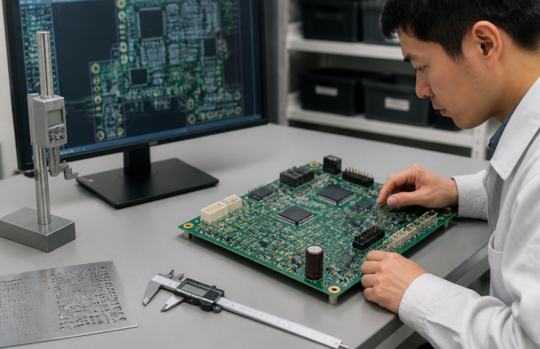
The PCB layout therefore needs to consider both technologies simultaneously.
Important design factors include:
- Through-hole diameter
- Pad size
- Component spacing
- Hole-to-copper clearance
- Soldering access
- Thermal distribution
- Component height
- Keep-out areas
The placement of through-hole components can also influence how efficiently the board moves through the production line.
Why Assembly Sequence Matters
One of the most interesting aspects of hybrid PCBA manufacturing is that the order of assembly can affect the entire production process.
Imagine a PCB containing hundreds of SMT components and several large THT connectors.
If the THT components are installed too early, they may interfere with automated SMT equipment or prevent the PCB from sitting properly on support tooling.
If they are installed too late, another manufacturing challenge may appear.
Therefore, engineers need to determine the optimal sequence.
A typical process may look like:
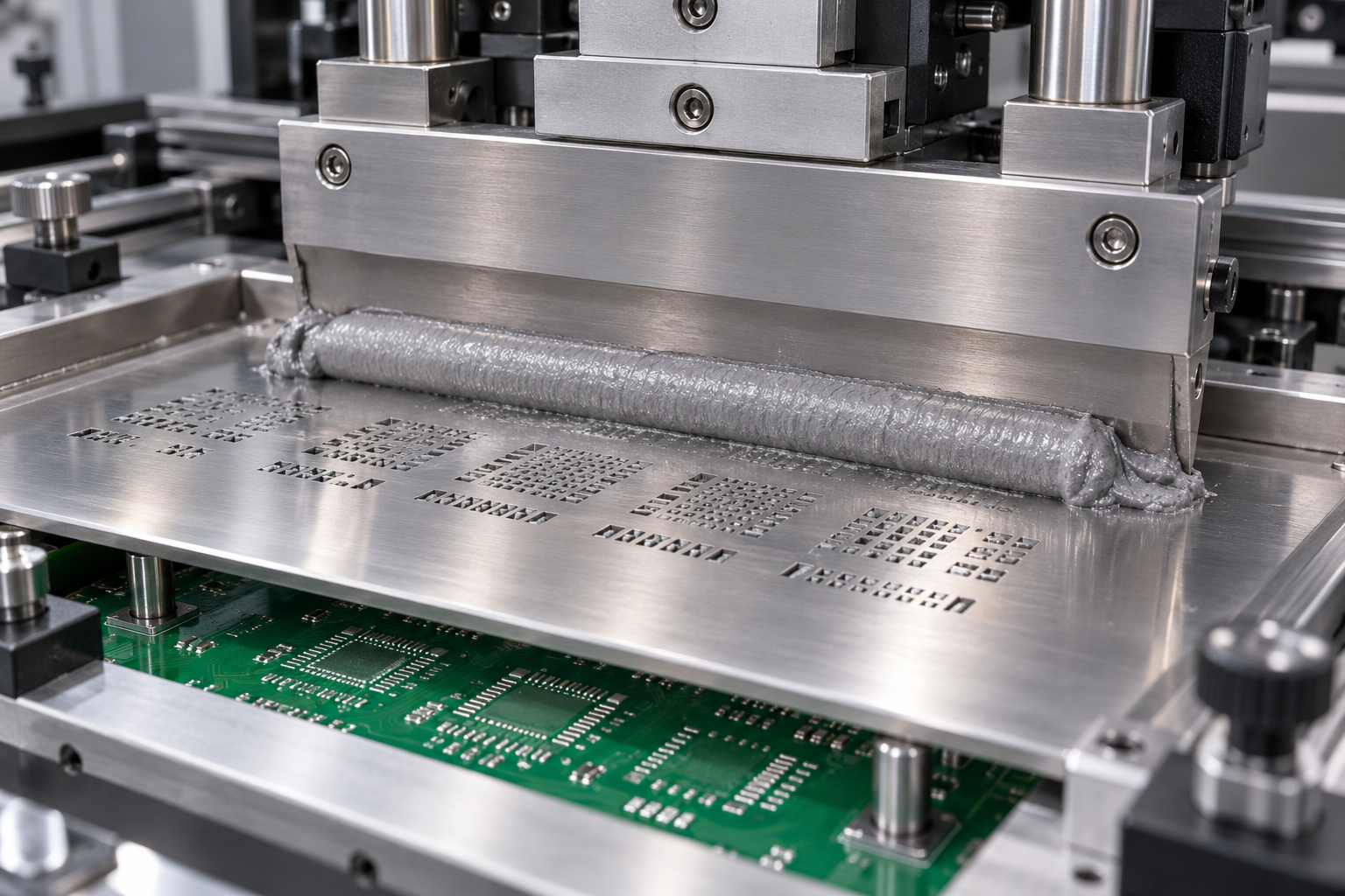
Solder Paste Printing → SPI → SMT Placement → Reflow → THT Insertion → Selective Soldering → AOI/X-Ray → Testing
However, the exact process depends on PCB structure, component selection, soldering requirements, and production volume.
There is no universal sequence for every hybrid PCBA.
 Selective Soldering Changes the Game
Traditional through-hole assembly often used wave soldering.
However, wave soldering is not always ideal for modern hybrid boards.
Why?
Because SMT components may already be populated on the opposite side of the PCB.
Passing the entire board through a solder wave can expose sensitive components to unnecessary solder contact.
This is where selective soldering becomes valuable.
Selective soldering applies molten solder only to specific through-hole locations.
The process can provide:
- Localized soldering
- Better process control
- Reduced solder exposure
- Compatibility with mixed SMT/THT assemblies
- Improved manufacturing flexibility
Instead of soldering the entire PCB, the machine targets specific through-hole joints.
This makes selective soldering especially useful for complex hybrid assemblies.
Wave Soldering vs. Selective Soldering
The choice between these processes depends on board design and production requirements.
Wave soldering can be highly efficient when a PCB contains many suitable through-hole joints arranged for wave processing.
Selective soldering becomes more attractive when:
- THT components are limited
- SMT components dominate the PCB
- Board geometry is complex
- Local soldering is required
- Thermal exposure needs to be minimized
Therefore, the PCB should ideally be designed with the intended soldering process in mind.
This is another example of how PCB design and PCBA manufacturing cannot be treated as completely separate activities.
Solder Pallets Become Important in Hybrid Assembly
Hybrid PCB assembly often requires specialized tooling.
A solder pallet or carrier can support the PCB during soldering and protect areas that should not be exposed to molten solder.
For example, a pallet may provide:
- PCB support
- Component protection
- Controlled solder exposure
- Improved board stability
- Consistent positioning
Tooling design becomes particularly important when the PCB contains a mixture of low-profile SMT components and tall THT components.
A well-designed carrier can make a significant difference in process stability.
Component Height Is More Than a Mechanical Specification
Component height may appear to be a simple dimensional parameter.
In hybrid assembly, however, it can affect the entire production sequence.
A tall connector or transformer may interfere with:
- Stencil printing
- Pick-and-place nozzles
- Conveyor systems
- Reflow oven clearance
- AOI cameras
- X-ray inspection
- Soldering fixtures
This means component height needs to be evaluated together with manufacturing equipment.
A component that fits perfectly inside the product enclosure may still create challenges on the production line.
Mixed Technology Creates Thermal Challenges
SMT and THT components may have very different thermal characteristics.
Large through-hole components can act as thermal masses.
Their metal leads and bodies may absorb heat differently from small SMT components.
During soldering, this can produce differences in:
- Heating rate
- Solder wetting
- Thermal equilibrium
- Cooling behavior
Large copper areas connected to through-hole pads can also draw heat away from the soldering region.
This becomes particularly important for high-current terminals and power components.
Engineers may therefore need to evaluate the PCB copper structure and thermal profile before mass production.
Why THT Holes Need Careful PCB Engineering
Through-hole components depend on drilled holes.
That introduces additional PCB fabrication requirements.
Engineers need to consider:
- Finished hole size
- Drill tolerance
- Plating thickness
- Annular ring
- Aspect ratio
- Component lead diameter
If the hole is too small, component insertion can become difficult.
If the hole is excessively large, solder filling and joint formation may be affected.
For plated through holes, the copper barrel also becomes part of the electrical connection.
Therefore, the hole is not simply an opening in the PCB.
It is part of the complete electrical and mechanical structure.
Hybrid Assembly and PCB Layer Design
Multilayer PCBs add another layer of complexity.
Through-hole drilling can pass through multiple PCB layers.
Engineers must ensure that the hole does not unintentionally interfere with:
- Power planes
- Ground planes
- High-speed signals
- Controlled impedance structures
- Internal copper regions
For some designs, non-functional pads may be removed where appropriate to improve manufacturability.
However, every change must be evaluated against electrical, mechanical, and manufacturing requirements.
This is why THT design should be considered during the PCB stack-up and layout stage rather than added at the end.
The Hidden Impact on SMT Process Efficiency
Hybrid assembly is not only about adding a THT step.
The presence of through-hole components can affect the efficiency of the entire SMT process.
For example, component placement may need to leave specific areas open.
Support pins may need to be positioned differently.
The board may require a customized carrier.
AOI inspection parameters may need additional programming.
Testing fixtures may also need to accommodate larger components.
As a result, hybrid assembly should be planned as an integrated manufacturing workflow.
Inspection Becomes More Complex
A hybrid PCBA contains different types of solder joints.
SMT joints may include:
- QFP leads
- QFN terminals
- BGA solder balls
- Passive component joints
THT joints may include:
- Connector pins
- Transformer leads
- Terminal blocks
- Large component leads
Different joints require different inspection approaches.
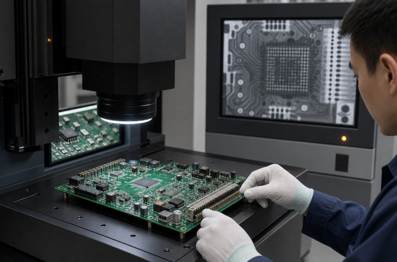
AOI can provide strong coverage for visible SMT solder joints.
X-ray inspection can reveal hidden solder connections such as BGA joints and certain internal structures.
For THT soldering, visual inspection and automated inspection can evaluate solder coverage and joint formation depending on the process.
The key is to match inspection technology with the physical characteristics of the joint.
Hybrid PCBA and Functional Testing
After assembly, the PCB still needs to perform its intended electrical functions.
Depending on the application, manufacturers may use:
- ICT
- Flying Probe Testing
- Functional Testing
- Programming
- Power-up testing
- Communication testing
- Burn-in testing
The presence of large THT components can sometimes influence fixture design.
For example, a connector may need to be accessible for functional testing.
This means test accessibility should be considered during PCB layout.
A beautifully assembled PCB can still create unnecessary production problems if its critical test interfaces are inaccessible.
When Should Engineers Choose Hybrid Assembly?
Hybrid assembly is particularly useful when the product combines high-density electronics with mechanical or power requirements.
Typical applications include:
- Industrial controllers
- Automation equipment
- Power control systems
- Communication equipment
- Automotive electronics
- Robotics
- Instrumentation
- Consumer appliances
In these applications, SMT can provide the required electronic density while THT provides additional mechanical or electrical robustness where needed.
 The Future Is Not SMT vs. THT
The future of PCBA manufacturing is unlikely to be about completely replacing one assembly technology with another.
Instead, the direction is toward technology integration.
A modern PCB may combine:
0201 + BGA + QFN + THT Connector + Power Device + Programming + Functional Testing
All of these technologies can coexist on the same assembly.
The manufacturing challenge is to create a process that treats them as one system rather than separate operations.
This requires cooperation between:
- PCB designers
- Component engineers
- SMT engineers
- THT process engineers
- Quality engineers
- Test engineers
The better these teams coordinate, the easier it becomes to build a stable production process.
SMT has transformed electronics manufacturing, but it has not eliminated the need for through-hole technology.
Instead, modern PCBA manufacturing is increasingly using both technologies where they make the most engineering sense.
SMT provides density and automation.
THT provides mechanical strength and flexibility.
Selective soldering connects the two manufacturing worlds.
The result is a hybrid PCBA process capable of supporting products that demand both compact electronic integration and reliable mechanical connections.
The real question is therefore not whether SMT or THT is better.
It is:
How can both technologies be engineered together to create a more manufacturable, reliable, and scalable PCBA?
As electronic products continue to combine miniaturized circuitry, high-power devices, mechanical interfaces, and complex control functions, hybrid PCB assembly will remain an important manufacturing strategy.
The smartest PCBA design is not necessarily the one that uses the newest technology everywhere.
It is the one that uses the right technology in the right place.

Leave A Comment