
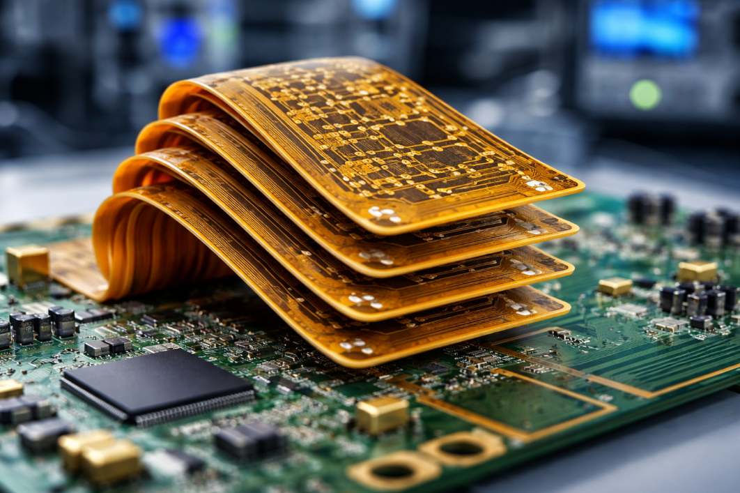
Unlocking the Future of Electronics Design: How 6-Layer Semi-Flex PCBs Are Reshaping Advanced Applications
1. The Evolution from Rigid to Flexible Technologies
In modern electronics manufacturing, PCB (Printed Circuit Board) technology is rapidly evolving from traditional rigid structures toward flexible and semi-flexible designs. With increasing demand for high density, miniaturization, and complex mechanical integration, semi-flex PCBs have become a preferred solution for engineers and product designers.
Compared with conventional rigid PCBs and fully flexible FPCs (Flexible Printed Circuits), semi-flex PCBs achieve a balance between structure and performance by enabling flexibility only in specific areas. This article focuses on the application of 6-layer semi-flex PCBs used for mainboard installation, covering materials, manufacturing processes, design considerations, and industry applications.
 2. What Is a 6-Layer Semi-Flex PCB?
2.1 Definition of Semi-Flex PCB
A semi-flex PCB is based on a rigid FR4 substrate, where specific areas are made flexible by reducing thickness or selectively removing rigid material. This is typically achieved through mechanical milling or laser processing to create flexible zones within an otherwise rigid board.
2.2 6-Layer Structure Overview
A typical 6-layer semi-flex PCB includes the following stack-up:
- Top Layer (Signal Layer)
- Inner Layer 1 (Power Plane)
- Inner Layer 2 (Signal Layer)
- Inner Layer 3 (Signal Layer)
- Inner Layer 4 (Ground Plane)
- Bottom Layer (Signal Layer)
This structure ensures strong signal integrity while providing sufficient routing space for complex and high-speed designs.
2.3 Comparison with Traditional Solutions
When comparing different PCB solutions, several key aspects highlight their differences.
In terms of cost, rigid PCBs are the most economical, while FPCs are the most expensive due to complex materials and processes. Semi-flex PCBs fall in between, offering a balanced cost-performance ratio.
Regarding flexibility, rigid PCBs cannot bend at all, FPCs support full dynamic bending, and semi-flex PCBs allow controlled bending in specific regions, making them ideal for structural applications.
In terms of reliability, rigid PCBs provide stable performance, FPCs may face fatigue risks under repeated bending, while semi-flex PCBs generally offer higher long-term reliability due to controlled flex zones.
From an application perspective, rigid PCBs are widely used in standard electronics, FPCs are common in wearable devices, and semi-flex PCBs are best suited for complex, space-constrained, and high-end electronic products.
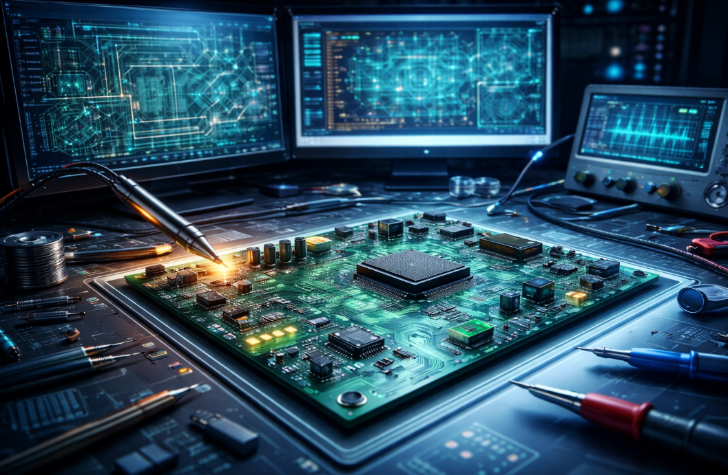 3. Materials and Manufacturing Processes
3.1 Core Material Selection
The performance of a 6-layer semi-flex PCB heavily depends on material selection. Common materials include:
- FR4 substrate: provides structural rigidity
- Polyimide (PI): used in flexible areas
- Adhesives: ensure strong layer bonding
Polyimide is particularly important due to its excellent thermal resistance (up to 260°C) and flexibility.
3.2 Manufacturing Process Flow
The manufacturing process of semi-flex PCBs is more complex than standard PCBs. Key steps include:
- Multilayer lamination
- Drilling and plating
- Imaging and pattern transfer
- Local thinning (back drilling or milling)
- Surface finishing (e.g., ENIG)
Among these, local thinning is the most critical step, directly affecting flexibility and reliability.
3.3 Key Technical Challenges
- Stress control in copper layers within bending areas
- Risk of delamination
- Micro-crack prevention
- Stable impedance control
 4. Design Considerations and Engineering Optimization
4.1 Flex Area Design Rules
When designing a 6-layer semi-flex PCB, the bending area must follow these guidelines:
- Minimum bend radius ≥ 10 times the board thickness
- Avoid vias in bending regions
- Use arc traces instead of sharp angles
4.2 Stack-Up Optimization
A well-designed stack-up significantly improves performance:
- Symmetrical structures reduce warpage
- Tight coupling of power and ground layers minimizes EMI
- Differential pair routing supports high-speed signals
4.3 Signal Integrity and EMC
The 6-layer structure provides clear advantages in high-speed applications:
- Controlled impedance (50Ω/100Ω)
- Reduced crosstalk
- Improved signal integrity (SI)
Proper grounding strategies also enhance electromagnetic compatibility (EMC).
5. Typical Application Scenarios
5.1 Industrial Control Systems
Semi-flex PCBs can replace traditional wire harnesses in complex mechanical systems, improving reliability and reducing assembly costs.
5.2 Medical Electronics
Devices such as endoscopes and portable monitoring equipment require both reliability and structural flexibility.
5.3 Automotive Electronics
In ADAS systems and in-vehicle cameras, semi-flex PCBs enable space optimization and improved vibration resistance.
5.4 Consumer Electronics
Applications like foldable devices and wearable electronics benefit from higher space utilization and compact integration.
6. Advantages in Mainboard Installation
6.1 Improved Space Utilization
The ability to bend allows the PCB to fit into complex mechanical structures, reducing the need for connectors.
6.2 Enhanced Reliability
Compared with FPC connections, semi-flex PCBs reduce the number of interconnects, lowering failure rates.
6.3 Balanced Cost and Performance
Semi-flex PCBs deliver performance close to FPCs while maintaining lower overall costs.
7. Future Development Trends
Driven by 5G, AIoT, and new energy vehicles, the demand for semi-flex PCBs continues to grow. Future trends include:
- Higher layer counts (8+ layers)
- Thinner polyimide materials
- Increased manufacturing automation for better yield
Combined with HDI (High Density Interconnect) technology, semi-flex PCBs will play an increasingly critical role in advanced electronics.
The 6-layer semi-flex PCB represents an innovative solution that combines the advantages of rigid and flexible technologies, redefining the boundaries of electronic design. From material selection to process control and design optimization, every stage reflects high engineering complexity and technical value.
For PCB and PCBA manufacturers, mastering semi-flex PCB technology is not only a way to enhance competitiveness but also a key step toward high-end manufacturing. As electronic design continues to push limits, semi-flex PCBs will undoubtedly become an essential core technology.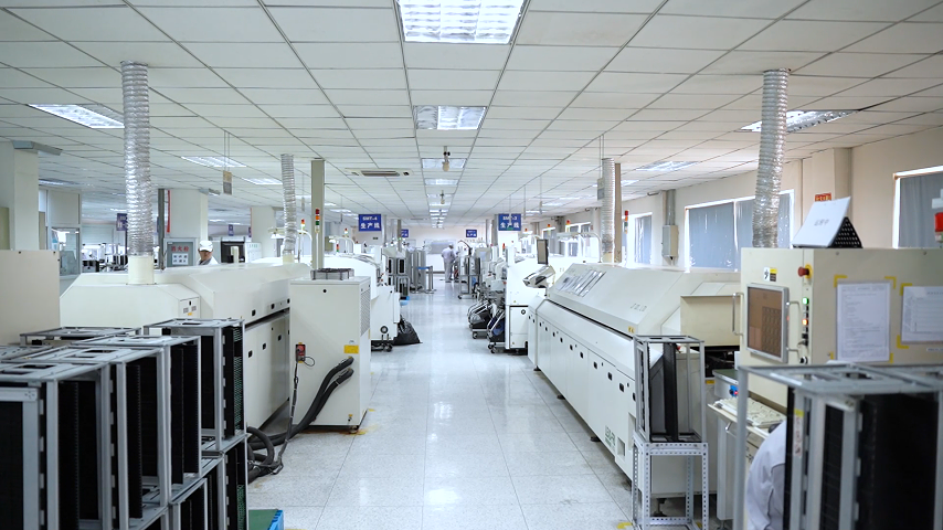

Leave A Comment