

What Are the Differences Between HDI and Non-HDI PCBs?
Introduction
Printed circuit boards (PCBs) play a crucial role in the design and manufacturing of electronic devices. As technology continues to advance, High-Density Interconnect (HDI) PCBs have emerged as a solution for creating smaller and more powerful electronic devices. HDI PCBs are known for their high density and complex circuit designs, enabling more functionality in a compact space compared to standard PCBs. But what are the specific differences between HDI and regular PCBs? In this article, we will explore various aspects to help readers understand the distinctions and their suitability in practical applications.
What is HDI PCB?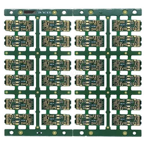
HDI PCBs are printed circuit boards based on high-density interconnect technology. They use small vias, blind vias, and buried vias to create more interconnections in a limited space, enhancing circuit board performance. The key features of HDI PCBs include high-density routing, multi-layer interconnects, high-frequency signal transmission, and smaller size. Because of these characteristics, HDI PCBs are widely used in modern electronic devices, especially in smartphones, tablets, and wearables that require miniaturization and high performance.
Main Differences Between HDI and Standard PCBs
Size and Weight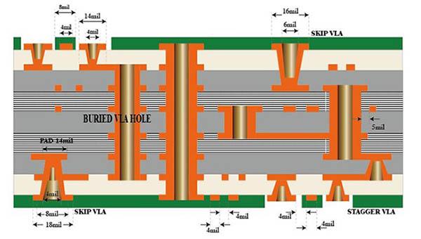
One of the notable advantages of HDI PCBs is their smaller size and lighter weight. HDI PCBs are designed to compress more circuitry into a smaller space compared to regular PCBs. This provides significant advantages for devices that are sensitive to volume and weight, such as mobile phones, laptops, and portable medical devices. Standard PCBs, on the other hand, are typically used in larger devices or applications that do not require a compact design.
Routing Density
Routing density is another key differentiator between HDI and standard PCBs. HDI PCBs use smaller traces and higher-density pads, allowing more circuits to be arranged in a limited space. They achieve multi-layer connections through the use of blind, buried, and micro vias, which are advanced manufacturing techniques. In contrast, standard PCBs have lower routing density and typically do not require the use of complex blind or buried vias.
Electrical Performance
HDI PCBs excel in electrical performance, especially in high-frequency and high-speed signal transmission. The shorter traces and compact design of HDI PCBs significantly reduce signal loss, improving signal integrity. As a result, HDI PCBs are widely used in applications requiring high data transfer rates, such as 5G communication devices, high-speed computers, and data centers. In contrast, standard PCBs perform well in low-frequency, simple signal transmission, but are less efficient in high-speed applications.
Via Technology
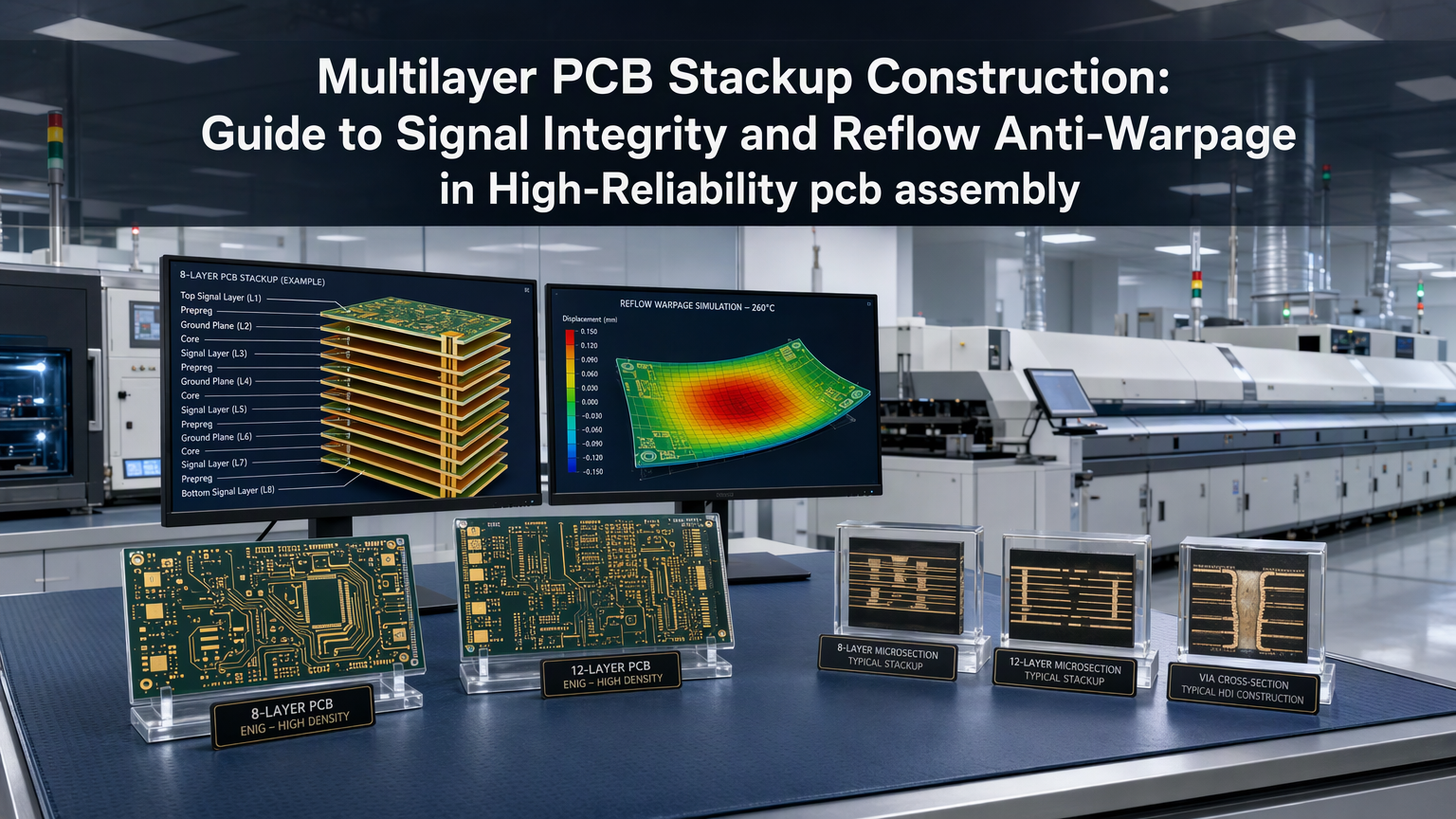
HDI PCBs are more sophisticated in terms of via technology compared to standard PCBs. They typically use blind, buried, and micro vias to connect multiple layers of circuitry, which reduces the distance between layers and increases layer density. This allows HDI PCBs to maintain high performance in complex multi-layer designs. Standard PCBs, on the other hand, primarily use through-hole vias and are suitable for simpler designs with fewer layers.
Applications of HDI PCBs
Due to their unique advantages, HDI PCBs are used in various high-performance and miniaturized electronic devices. Here are some common applications:
- Smartphones and Tablets: HDI PCBs are essential in modern mobile devices, helping them achieve slim designs and high efficiency.
- Medical Devices: In portable and miniaturized medical equipment, HDI PCBs offer compact designs and precise signal transmission to ensure reliability.
- Automotive Electronics: With the increasing intelligence of automotive electronic systems, HDI PCBs play an important role in automotive navigation and autonomous driving systems.
- High-Performance Computing: Servers, data centers, and supercomputers require high-speed signal processing, and HDI PCBs excel in these fields.
Manufacturing Process of HDI PCBs
Via-in-Pad Process
One of the key technologies in HDI PCB manufacturing is the via-in-pad process. This technique allows multiple pads and circuits to be connected with high density, using filled vias. These filled pads can be used for wiring on other layers or for support, enhancing the overall stability and performance of the HDI PCB.
Lamination and Material Process
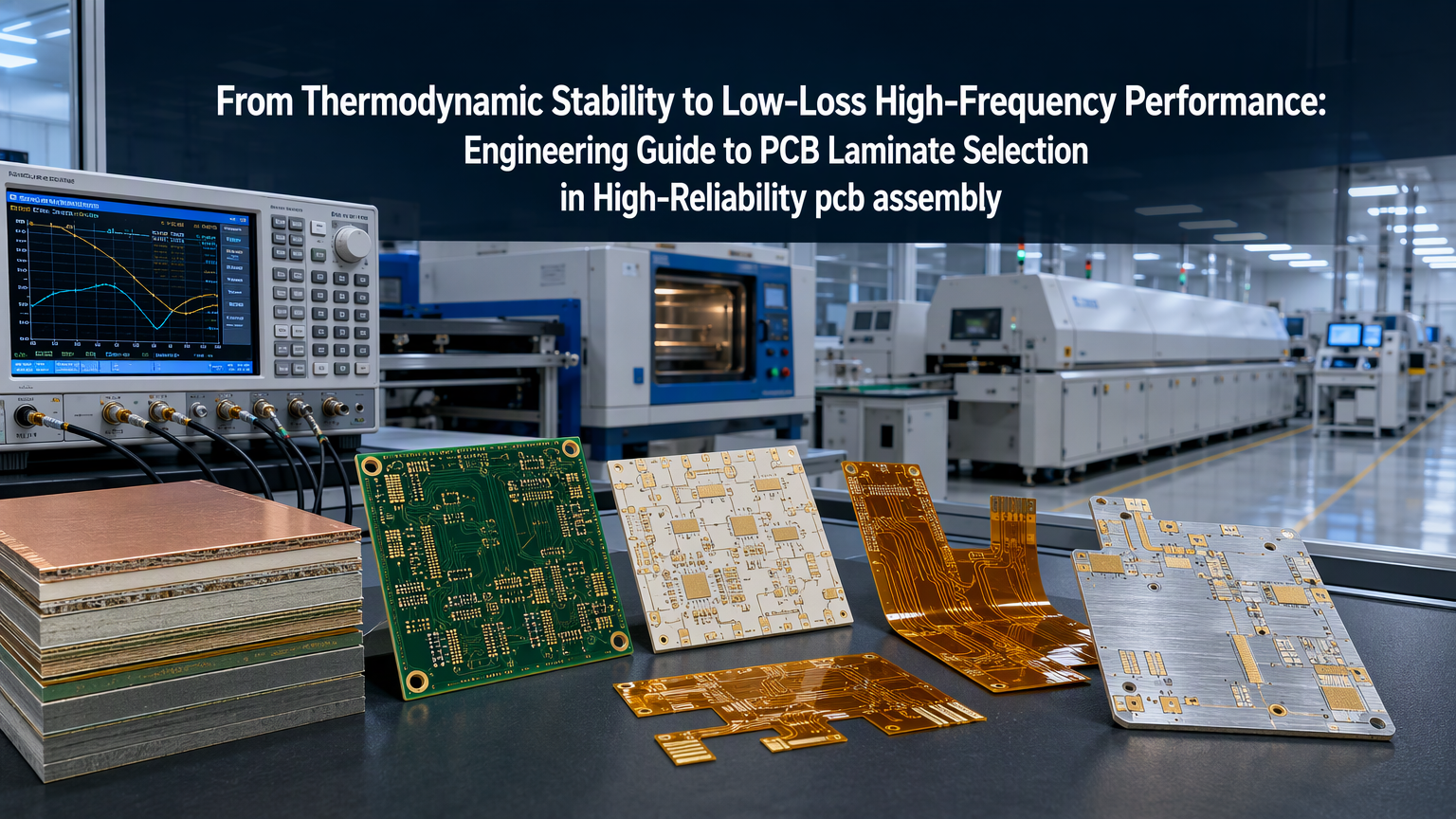
Lamination is a crucial step in the manufacturing of HDI PCBs. This process involves stacking and bonding multiple PCB layers to form a multi-layer structure. HDI PCBs often require multiple lamination cycles to complete. The process not only requires precise alignment but also uses special materials to ensure the electrical performance and mechanical strength of each layer.
Advantages of HDI PCBs
- Greater Design Flexibility: HDI PCBs allow designers to implement more complex circuits in limited space, offering more design freedom.
- Superior Electrical Performance: HDI PCBs offer shorter signal paths and reduced signal loss, enhancing signal integrity, particularly in high-speed data transmission applications.
- Miniaturization and Lightweight: The high-density design of HDI PCBs makes them suitable for small devices such as portable electronics and wearables.
- Improved Durability: Through advanced manufacturing processes, HDI PCBs offer better resistance to heat, shock, and long-term use, making them ideal for industrial-grade equipment.
Cost Comparison Between HDI and Non-HDI PCBs
Despite the clear advantages of HDI PCBs, their manufacturing cost is generally higher than that of standard PCBs. This is due to the more complex manufacturing processes and the need for high-precision equipment. However, while the initial manufacturing cost of HDI PCBs may be higher, their benefits in terms of signal performance, design flexibility, and size make them more cost-effective in applications with high demands.
Conclusion
HDI PCB and ordinary PCB each have different advantages and application areas. For products that require high-density wiring, high-performance signal transmission and miniaturized design, HDI PCB is undoubtedly the best choice. For electronic products with simpler requirements, ordinary PCB is still the most cost-effective solution. The final choice of PCB depends on the needs and budget of the specific application. To understand the difference between the two and get a more favorable quotation, please contact us. We have a professional technical team to give you a detailed quotation

Leave A Comment