

When PCB Printing Meets High-Precision Manufacturing: Can It Truly Meet Real-World Demands for Accuracy, Reliability, and Consistency?
In the field of electronics manufacturing, the term “PCB printing” typically refers to solder paste printing or conductive ink printing processes. It is a critical front-end step in the SMT (Surface Mount Technology) workflow. As electronic products continue to evolve toward higher density, miniaturization, and high-frequency/high-speed performance, the precision, reliability, and consistency of PCB printing have become decisive factors affecting PCBA yield and long-term stability.
So, in real-world production environments, can PCB printing truly meet industrial-grade application requirements? This article provides a systematic analysis from four dimensions: precision control, process stability, reliability assurance, and mass-production consistency.
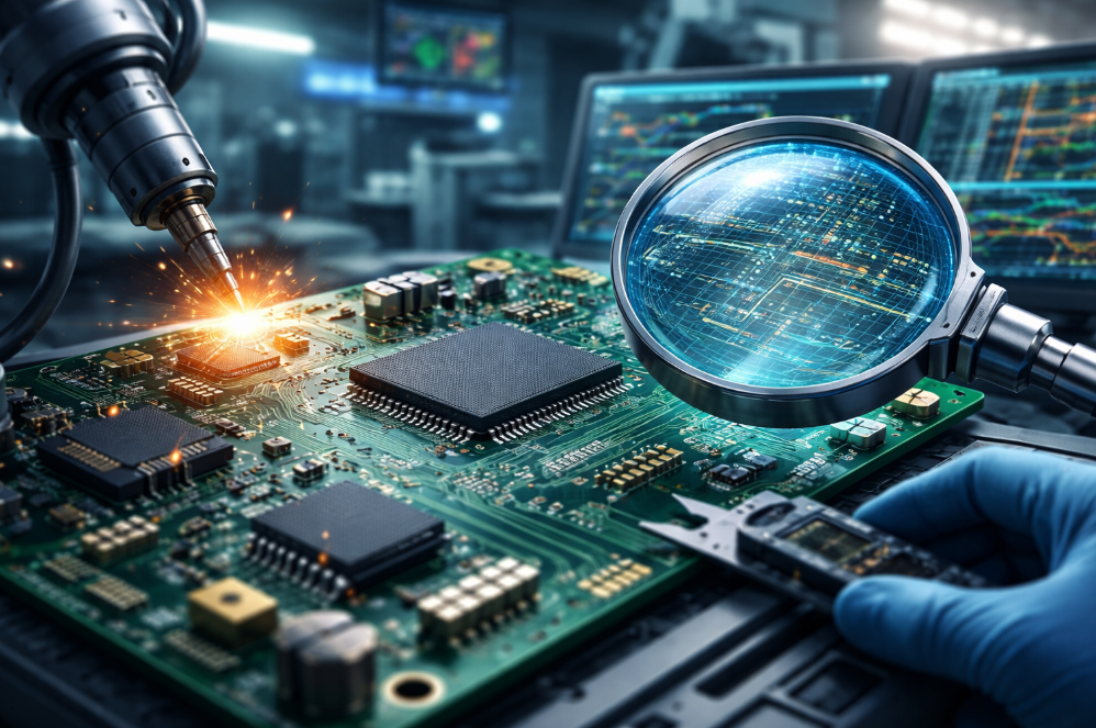 1. The Technical Nature and Process Role of PCB Printing
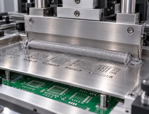
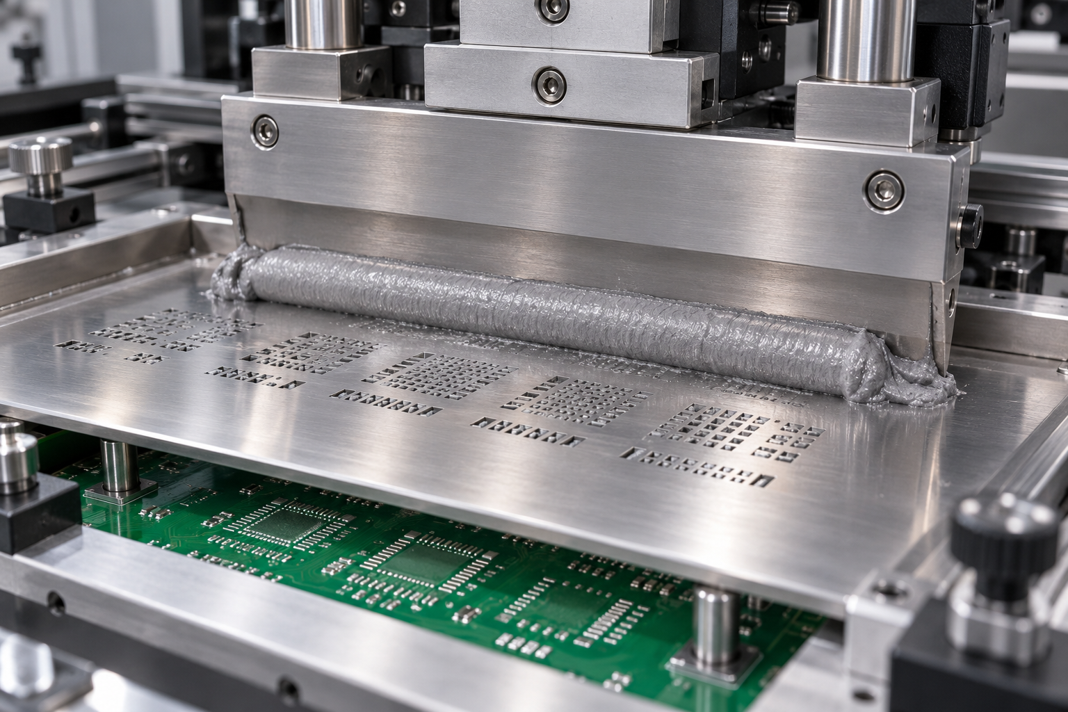
PCB printing is far more than a simple “coating” procedure. Through the coordinated action of a stencil and squeegee system, solder paste or conductive materials are transferred onto PCB pads with controlled thickness and volume. This process directly affects the following key parameters:
- Solder volume
- Pad coverage
- Paste slump behavior
- Risk of solder bridging
- Post-reflow void rate
In applications such as HDI boards, 0.4 mm pitch QFN, fine-pitch BGA, and even 01005 components, printing deviations are often controlled at the micron (μm) level. Therefore, the precision capability of PCB printing directly determines the success rate of subsequent placement and reflow soldering processes.
2. Precision Dimension: How Accurate Can PCB Printing Be?
2.1 Stencil Design Defines the Theoretical Precision Ceiling
Stencil thickness, aperture design, electro-polishing processes, and nano-coating technologies all influence paste release rate.
In mature production environments:
- Printing alignment accuracy can be controlled within ±12.5 μm
- Solder paste volume deviation can be maintained within ±10%
- SPI (Solder Paste Inspection) enables 100% inspection coverage
With step stencil design, manufacturers can simultaneously accommodate large power devices and ultra-fine-pitch chips on the same PCB, ensuring optimized solder deposition across varying component requirements.
2.2 Equipment Capability and Automatic Compensation Systems
Modern fully automatic stencil printers are equipped with:
- Vision alignment systems
- Closed-loop pressure control
- Under-stencil cleaning systems
- Temperature and humidity monitoring modules
These technologies ensure micron-level repeatability even in high-speed mass production.
Conclusion: Under standard industrial conditions, PCB printing can fully meet the precision requirements of high-end electronic products—provided that process parameters and equipment maintenance are properly managed.
 3. Reliability Dimension: How Printing Quality Impacts Long-Term Performance
3.1 Solder Joint Structure and Mechanical Strength
Insufficient paste deposition can result in cold solder joints, while excessive volume increases the risk of bridging and void formation. Proper solder paste deposition forms uniform intermetallic compounds (IMC), enhancing shear strength and thermal cycling stability.
3.2 Thermal Cycling and Fatigue Life
In automotive electronics, industrial control systems, and communication equipment, PCBs may experience temperature cycling from -40°C to 125°C. Printing uniformity directly influences stress distribution across solder joints.
The higher the volume consistency, the lower the probability of fatigue crack formation.
3.3 Void Rate Control
For power devices such as MOSFETs and IGBTs, a void rate below 25% is generally considered acceptable. High-quality printing significantly reduces gas entrapment and void formation during reflow.
Conclusion: When combined with SPI inspection and optimized reflow profiling, PCB printing can meet stringent industrial reliability standards.
4. Consistency Dimension: The Real Challenge of Mass Production
While printing precision is relatively manageable in small-batch prototyping, consistency becomes the defining factor in large-scale mass production.
4.1 Key Factors Affecting Consistency
- Solder paste viscosity drift
- Environmental temperature and humidity fluctuations
- Squeegee wear
- Stencil contamination
Even minor variables can escalate into large-scale defects during continuous production.
4.2 SPC and Data-Driven Process Management
Advanced manufacturing facilities typically implement:
- Statistical Process Control (SPC)
- CPK analysis
- Real-time SPI data tracking
- MES-based closed-loop management
Through data-driven monitoring and optimization, printing defect rates can be reduced to PPM-level performance.
Conclusion: The consistency of PCB printing is not a standalone capability—it reflects the overall maturity of the manufacturing system.
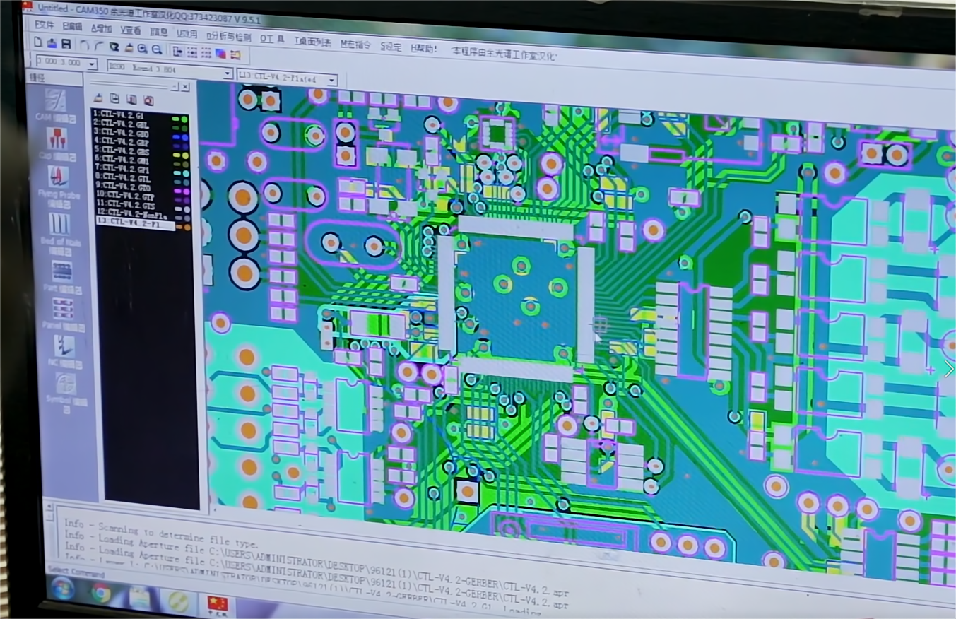 5. Limitations and Future Optimization of PCB Printing
Despite its maturity, PCB printing still faces technical challenges:
- Ultra-fine-pitch components demand higher solder powder grades (Type 4/5/6).
- Ultra-thin PCBs are prone to warpage, affecting stencil contact stability.
- High-frequency substrates impose stricter requirements on solder joint integrity.
Future optimization directions include:
- Nano-coated stencils
- Jet printing technology
- AI-driven parameter optimization systems
- End-to-end digital process integration
6. Comprehensive Evaluation: Can PCB Printing Meet Real-World Application Needs?
From the perspectives of precision, reliability, and consistency, PCB printing in a modern automated SMT environment is fully capable of supporting consumer electronics, industrial control, automotive electronics, and communication equipment applications.
What ultimately determines whether it “meets the standard” is not a single piece of equipment, but rather:
- Process engineering capability
- Quality control systems
- Data-driven management
- Standardized operations and continuous optimization mechanisms
In other words, PCB printing itself is not the bottleneck—system-level manufacturing excellence is the true determinant.
From a Simple Printing Step to a Source of Quality Control
In today’s high-reliability electronics manufacturing landscape, PCB printing is no longer just a front-end process. It has evolved into a critical source control point that directly determines the stability and yield of finished PCBA products.
When companies integrate precision stencil design, advanced automation equipment, full SPI inspection, and SPC-based data management into a closed-loop system, PCB printing not only meets real-world application requirements but also becomes a strategic lever for enhancing product competitiveness.
For manufacturers pursuing high yield rates and long-term reliability, optimizing PCB printing is not merely a cost investment—it is a strategic investment in quality.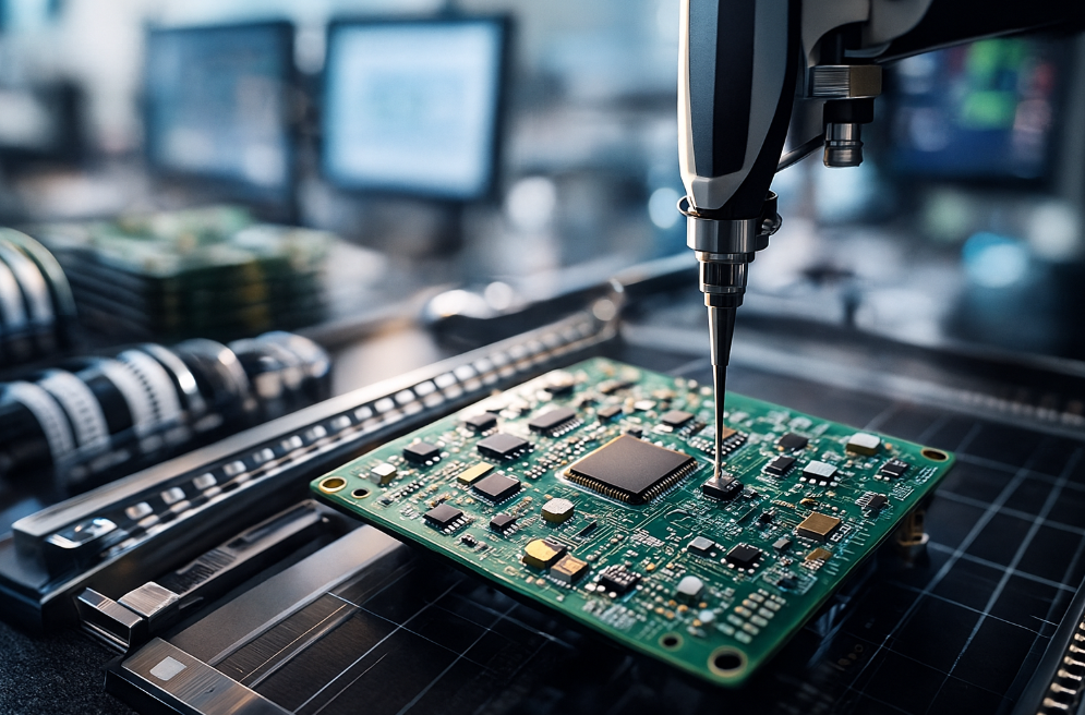

Leave A Comment