

When the PCB Bends, PCBA Fails: How Board Warpage Affects SMT Assembly and Reliability
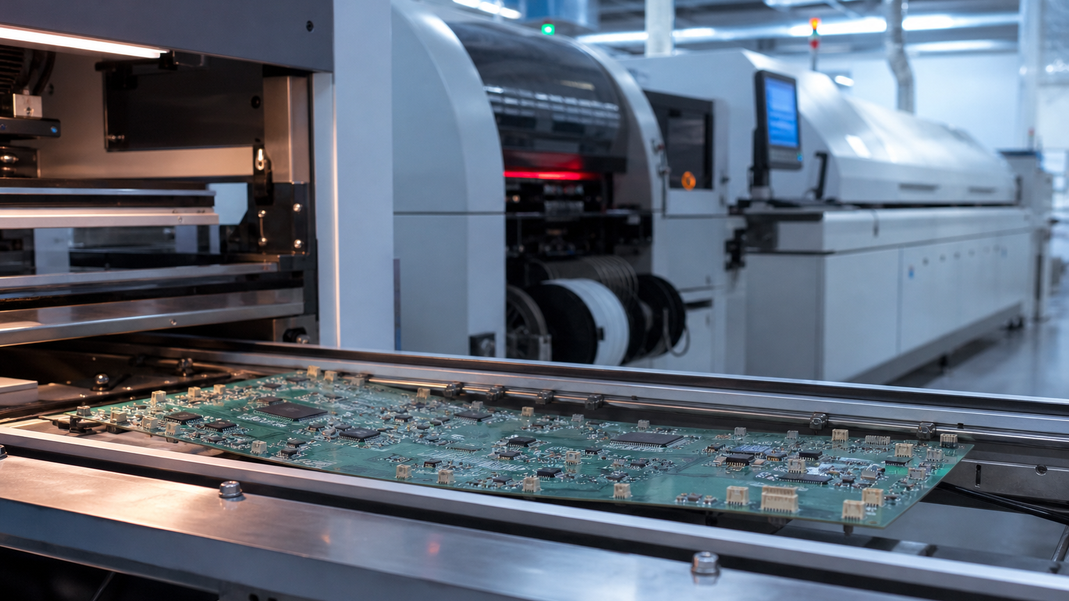
A PCB can look perfect when it leaves the fabrication line, yet behave very differently once it enters SMT assembly. During solder paste printing, component placement, and reflow soldering, even a small amount of board warpage can create problems that are difficult to trace back to the original cause.
This is why PCB warpage is more than a mechanical issue. It can directly influence SMT assembly accuracy, solder joint quality, BGA reliability, production yield, and long-term PCBA performance.
As electronic products become thinner, more compact, and increasingly populated with fine-pitch components, controlling PCB flatness has become an important part of modern PCBA manufacturing.
 What Is PCB Warpage?
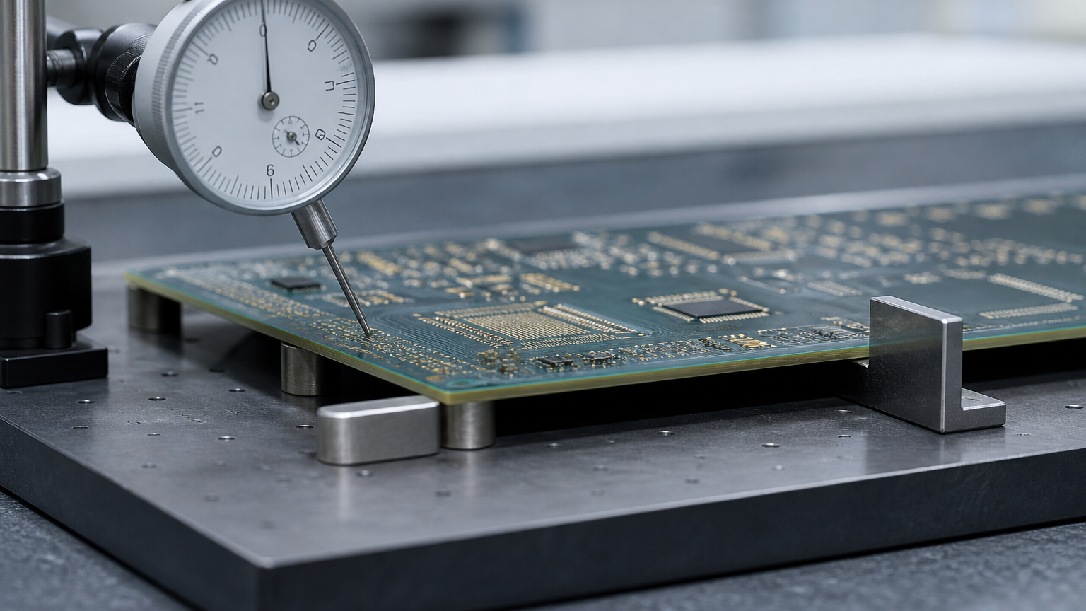
PCB warpage refers to the unwanted deformation of a printed circuit board from its intended flat geometry.
In practical manufacturing, warpage may appear as:
- Bow, where the PCB bends gradually across its surface
- Twist, where different corners of the PCB move in different directions
- Local deformation around dense copper areas
- Edge lifting after thermal processing
- Dimensional deformation caused by repeated heating and cooling
A PCB does not necessarily need to be visibly bent to create an assembly problem. At the SMT level, a relatively small deformation can change the distance between the stencil, PCB pads, and component leads.
This becomes especially important for fine-pitch QFP, QFN, CSP, BGA, and micro-BGA packages.
The key point is simple:
PCB flatness is part of the assembly process, not just a cosmetic requirement for the bare board.
 Why Does PCB Warpage Happen?
PCB warpage usually comes from a combination of material properties, copper distribution, layer construction, manufacturing processes, and thermal stress.
1. Uneven Copper Distribution
Copper is not only an electrical conductor. It also affects the mechanical behavior of the PCB.
Consider a multilayer board where one area contains large copper planes while the opposite side contains relatively little copper. During lamination and thermal cycling, the two sides may respond differently.
This imbalance can contribute to internal stress and eventually produce board deformation.
For complex PCBs, engineers therefore need to consider copper balance during stack-up and layout development.
2. Multilayer Stack-Up Structure
The structure of a multilayer PCB has a major influence on mechanical stability.
Different combinations of:
- Core thickness
- Copper thickness
- Number of layers
- Resin content
- Dielectric materials
- can create different thermal and mechanical characteristics.
A symmetrical stack-up generally provides better mechanical balance than a highly asymmetric structure.
However, achieving symmetry is not always straightforward. High-density designs may require heavy copper layers, special dielectric materials, or mixed construction, making stack-up engineering more challenging.
3. Thermal Expansion
During PCBA production, the PCB may experience several thermal cycles.
For example:
PCB fabrication → solder paste printing → preheating → reflow → cooling → testing → rework
Each thermal cycle can introduce mechanical stress.
The coefficient of thermal expansion, or CTE, differs among copper, resin, laminate materials, solder, and electronic components.
When these materials expand and contract at different rates, mechanical stress can accumulate.
This is particularly important for multilayer boards and assemblies containing large packages.
 How PCB Warpage Affects SMT Assembly
The consequences of board deformation often begin during solder paste printing.
Solder Paste Printing
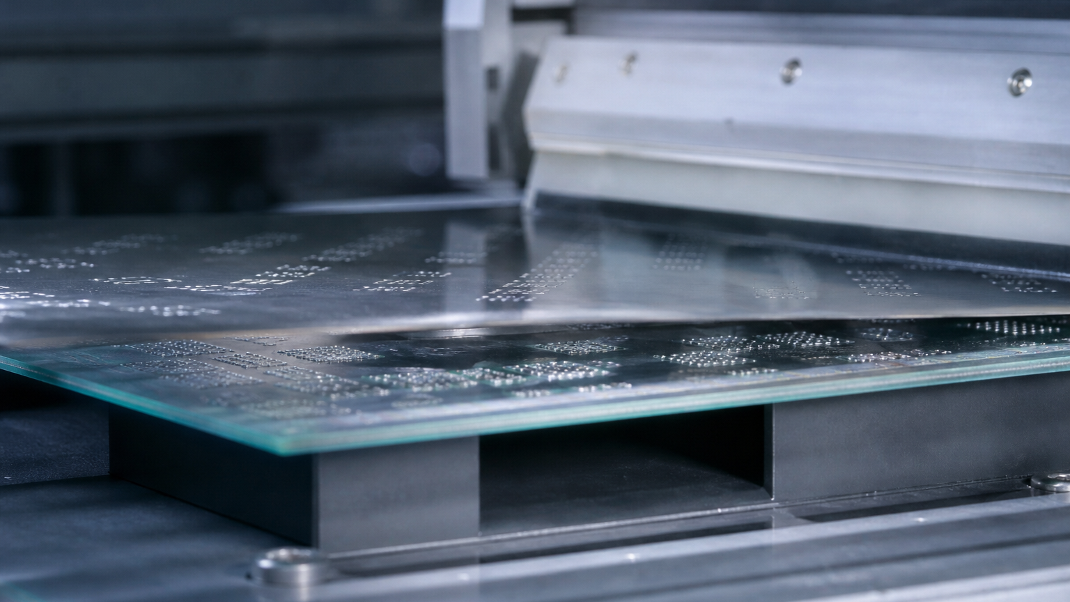
A stencil printing process relies on controlled contact between the stencil and the PCB surface.
If the board is warped, the PCB may not maintain uniform contact with the stencil.
This can lead to:
- Insufficient solder paste deposition
- Excessive solder paste
- Inconsistent paste volume
- Paste smearing
- Poor pad definition
- Increased risk of solder bridging
- For fine-pitch components, even a small change in solder paste volume can influence solder joint formation.
This is why modern PCBA production often combines precise printing parameters with SPI, or Solder Paste Inspection, to monitor solder paste height, area, volume, and offset.
However, SPI can identify the consequence of deformation; it does not automatically eliminate the mechanical cause.
PCB Warpage and Component Placement
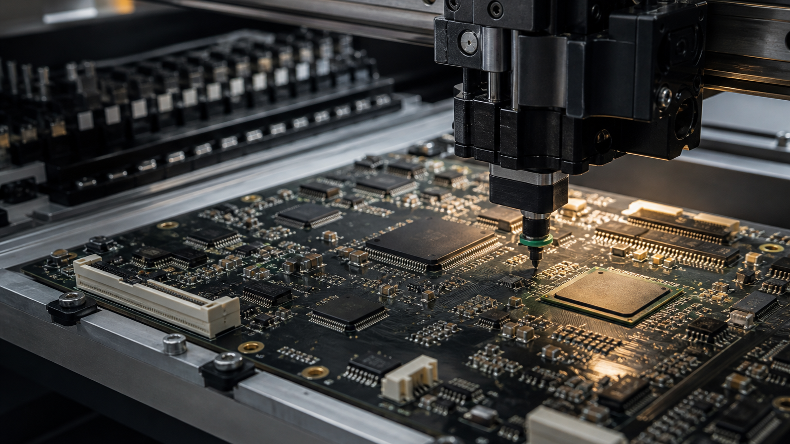
After solder paste printing, the PCB enters the pick-and-place process.
Modern SMT placement machines can achieve extremely high placement accuracy. But equipment accuracy cannot completely compensate for an unstable mechanical surface.
When the PCB is not sufficiently flat, several problems may occur:
- Component placement offset
- Uneven component seating
- Reduced placement repeatability
- Mechanical interference
- Increased risk for fine-pitch components
- This is especially significant when a single PCB combines different package technologies.
For example, a board may contain:
0201 passive components + QFN + fine-pitch QFP + BGA + connectors
Each package has different placement and soldering requirements.
The flatter and more stable the PCB surface is, the easier it becomes to maintain process consistency across the entire assembly.
 The Hidden Risk During Reflow Soldering
Reflow soldering is where PCB warpage can become even more complicated.
During reflow, the PCB is heated through several controlled zones until the solder paste reaches its melting temperature.
The board then enters the cooling stage.
This heating and cooling process can temporarily increase deformation.
A PCB that appears acceptable at room temperature may behave differently at elevated temperatures.
This creates an important engineering question:
Is the PCB flat only at room temperature, or does it remain mechanically stable throughout the reflow profile?
For high-density PCBA, the second question is often more meaningful.
Why BGA Components Are Particularly Sensitive
BGA packages are highly sensitive to PCB deformation because the solder joints are hidden underneath the component body.
Unlike visible gull-wing leads, BGA solder joints cannot be fully evaluated through conventional visual inspection.
If the PCB and BGA package experience different deformation during reflow, solder balls may not form uniform joints.
Potential problems include:
- Open solder joints
- Head-in-pillow defects
- Non-uniform solder joint geometry
- Excessive voiding
- Intermittent electrical connections
- Mechanical reliability problems
This is why X-ray inspection has become an important inspection method for assemblies containing BGA and other bottom-terminated components.
X-ray can help identify internal solder joint conditions that cannot be confirmed through conventional optical inspection.
PCB Thickness Also Matters
PCB thickness is another variable that should not be considered independently from assembly requirements.
A thin PCB may provide advantages for compact product design, but it can also be mechanically less rigid.
For larger board dimensions, the relationship between:
Board size + thickness + material + copper distribution + support method
becomes increasingly important.
A very large and thin PCB can be more susceptible to deformation during SMT processing than a smaller board with similar material construction.
Therefore, PCB mechanical design should be evaluated together with the intended PCBA manufacturing process.
How Manufacturers Can Reduce PCB Warpage
Controlling PCB warpage requires cooperation between PCB fabrication and PCBA assembly teams.
Optimize the PCB Stack-Up
A properly engineered stack-up can improve structural balance.
Important considerations include:
- Symmetrical layer arrangement
- Balanced copper distribution
- Appropriate core and prepreg selection
- Controlled dielectric thickness
- Suitable copper weights
- Stack-up optimization should happen during PCB design rather than after manufacturing problems appear.
Improve Copper Balance
When large copper planes exist on one side of a board, engineers can evaluate whether copper distribution can be balanced on the opposite side.
This does not mean randomly adding copper.
Copper balancing must consider:
- Electrical clearance
- Thermal requirements
- Impedance requirements
- Current carrying capacity
- Signal integrity
- Manufacturing constraints
- Therefore, copper balance is an engineering optimization rather than a simple visual adjustment.
Control Reflow Temperature
The reflow profile should be matched to the solder paste, PCB construction, and component requirements.
A properly controlled profile helps minimize unnecessary thermal stress.
Key parameters include:
- Preheat rate
- Soak zone
- Time above liquidus
- Peak temperature
- Cooling rate
- The objective is not simply to reach the required soldering temperature, but to create a controlled thermall process across the entire PCB assembly.
Mechanical Support During SMT
PCB support tooling can also help reduce deformation during assembly.
Depending on board geometry, manufacturers may use:
- Support pins
- Tooling fixtures
- Vacuum support
- Customized carriers
- Edge support systems
- Support becomes particularly important for large, thin, or irregularly shaped boards.
The correct support strategy can improve printing stability and placement repeatability while reducing mechanical stress during production.
Inspection Should Follow the Failure Mechanism
One of the most effective approaches to PCBA quality is to connect inspection technology with specific failure mechanisms.
For example:
PCB warpage → unstable printing → SPI
Placement variation → AOI
Hidden BGA solder defects → X-ray
Electrical performance → ICT/FCT
This creates a more complete manufacturing feedback loop.
Instead of treating inspection as a final pass/fail operation, manufacturers can use inspection data to identify where the process begins to drift.
PCB Warpage Is a System-Level Manufacturing Problem
An important lesson is that PCB warpage rarely belongs to only one manufacturing stage.
PCB fabrication influences the mechanical structure.
SMT printing interacts with board flatness.
Placement accuracy depends partly on board stability.
Reflow changes the thermal stress state.
Inspection reveals downstream defects.
Testing determines whether those defects affect electrical performance.
Therefore, the solution requires cooperation across the entire PCB and PCBA manufacturing chain.
A board designer may focus on electrical performance. A PCB manufacturer may focus on lamination and fabrication. An SMT engineer may focus on printing and placement. A quality engineer may focus on inspection.
But the final PCBA does not separate these disciplines.
The assembled board experiences all of them simultaneously.
From PCB Design to Reliable PCBA
The most effective way to manage PCB warpage is to address it before production.
During the engineering stage, manufacturers and customers can evaluate:
- PCB layer count and stack-up
- Board thickness and dimensions
- Copper distribution
- Material selection
- Component density
- BGA/QFN placement
- Reflow thermal requirements
- SMT support strategy
- Inspection requirements
- Functional testing conditions
This approach transforms PCB warpage from a reactive quality problem into a proactive manufacturing consideration.
For prototype production, the issue may first appear as inconsistent solder paste printing or component placement.
During volume production, however, a small mechanical variation can become a significant yield issue.
That is why early engineering review is valuable.
The Future of PCBA: Mechanical Stability Meets Process Intelligence
Modern PCBA manufacturing is becoming increasingly data-driven.
SPI, AOI, X-ray, placement machines, reflow ovens, and testing systems generate large amounts of process information.
The next step is connecting these datasets.
For example, if SPI repeatedly detects abnormal solder paste volume in a particular PCB region, engineers can compare that information with board deformation, copper distribution, support locations, and reflow behavior.
This creates a new manufacturing perspective:
A PCB is not simply a carrier for electronic components. It is a mechanical, thermal, and electrical structure operating inside a manufacturing process.
Understanding this relationship can help manufacturers identify problems earlier and improve overall assembly consistency.
PCB warpage may seem like a minor mechanical issue, but in advanced PCBA manufacturing, it can influence nearly every stage of the SMT process.
From solder paste printing and component placement to reflow soldering, BGA inspection, electrical testing, and long-term reliability, PCB flatness can become an invisible factor behind visible manufacturing defects.
The most reliable approach is not to wait until the assembled board fails inspection.
Instead, PCB structure, material selection, copper balance, stack-up symmetry, thermal behavior, SMT support, and inspection methods should be considered together from the beginning.
As electronic products continue to move toward thinner boards, higher component density, finer pitches, and more complex assemblies, mechanical stability will become an increasingly important part of PCBA engineering.
In other words, achieving reliable PCBA performance does not always begin with the component.
Sometimes, it begins with keeping the PCB flat.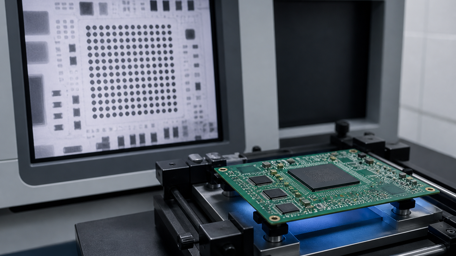








Leave A Comment