
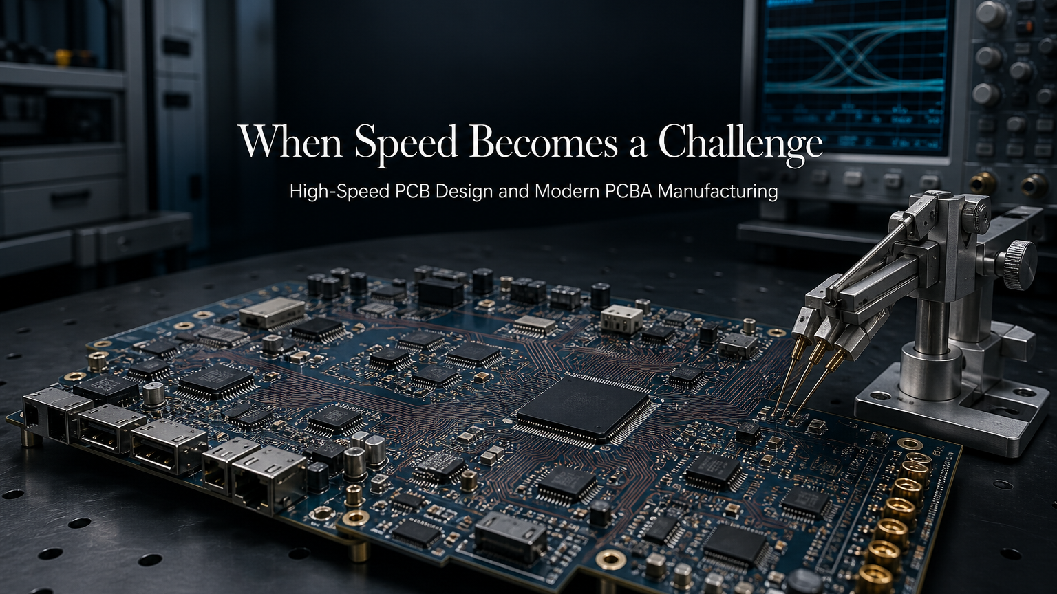
When Speed Becomes a Challenge: How High-Speed PCB Design Is Reshaping Modern PCBA Manufacturing
The Faster Electronics Become, the Less Room There Is for Error
Electronic products are moving faster than ever.
From industrial controllers and communication equipment to computing devices and intelligent hardware, modern systems increasingly rely on high-speed data transmission.
Interfaces such as USB, Ethernet, PCIe, DDR, HDMI, LVDS, and other high-speed protocols can transfer enormous amounts of data within extremely short periods.
But higher data rates create a new challenge for PCB and PCBA engineers.
A signal that behaves normally on a low-speed PCB may become distorted when the same circuit operates at high speed.
Unexpected problems may appear:
- Signal reflection
- Crosstalk
- Overshoot and undershoot
- Timing errors
- Electromagnetic interference
- Data corruption
- Intermittent communication failures
At this point, PCB design is no longer simply about connecting components with copper traces.
The PCB itself becomes part of the electrical system.
This is why high-speed PCB design and signal integrity have become critical considerations in modern PCBA development.
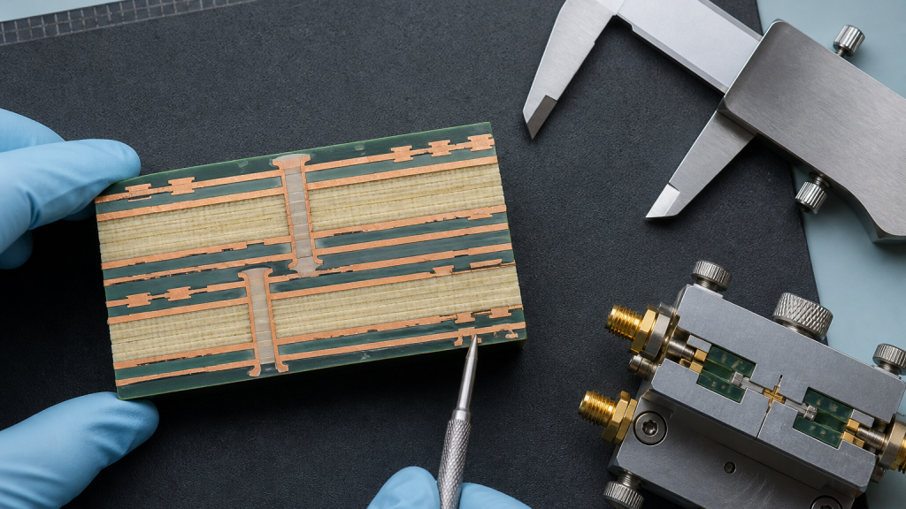 1. What Makes a PCB “High Speed”?
High-speed PCB design is not determined only by the clock frequency printed in a datasheet.
A better way to understand it is to consider the relationship between the signal transition time and the physical length of the PCB trace.
Even when the operating frequency does not appear extremely high, a fast signal edge can contain significant high-frequency components.
When the signal transition becomes sufficiently fast, the PCB trace behaves more like a transmission line than an ordinary wire.
This changes the design requirements.
Engineers may need to consider:
- Characteristic impedance
- Propagation delay
- Trace geometry
- Dielectric constant
- Reference planes
- Return current
- Differential routing
This is where conventional PCB layout practices begin to show their limitations.
2. The PCB Trace Is Part of the Signal Path
A common assumption is that the signal travels from one IC pin directly to another.
In reality, the signal path includes much more:
Driver → PCB Trace → Via → Connector → PCB Trace → Receiver
Every physical structure can influence signal behavior.
Trace width, copper thickness, dielectric thickness, PCB material, vias, connectors, and even reference-plane changes can introduce electrical discontinuities.
For low-speed signals, these effects may be negligible.
For high-speed signals, they can become significant.
This is why high-speed PCB design requires engineers to treat the physical PCB structure as part of the circuit.
 3. Why Controlled Impedance Matters
One of the most important concepts in high-speed PCB design is controlled impedance.
Characteristic impedance is influenced by several physical parameters, including:
- Trace width
- Trace thickness
- Dielectric thickness
- Dielectric constant
- Distance to the reference plane
Common PCB structures include:
- Microstrip
- Stripline
- Embedded microstrip
The objective is to maintain a predictable impedance along the signal path.
For example, a high-speed interface may require a specific single-ended or differential impedance according to its electrical specification.
If the impedance changes significantly along the route, signal reflections can occur.
4. What Causes Signal Reflection?
Imagine a signal traveling along a PCB trace.
If the signal encounters a sudden impedance discontinuity, part of the energy may be reflected back toward the source.
This can happen at:
- Incorrect trace geometry
- Vias
- Connectors
- Stubs
- Layer transitions
- Poorly designed pads
The resulting waveform may exhibit:
- Ringing
- Overshoot
- Undershoot
- Timing distortion
At lower speeds, these effects may not affect system operation.
At high data rates, however, they can reduce the available signal margin.
This is why maintaining a continuous and predictable transmission path is so important.
 5. Differential Pairs Need More Than Parallel Traces
Many modern communication interfaces use differential signaling.
A differential pair contains two traces carrying complementary signals.
Examples include:
- USB
- Ethernet
- PCIe
- LVDS
- CAN-related high-speed interfaces
- High-speed display interfaces
The two traces should generally be routed with controlled:
- Trace width
- Trace spacing
- Length relationship
- Reference-plane structure
The goal is to maintain consistent differential behavior.
If the two traces experience significantly different electrical environments, the differential signal can become unbalanced.
This may increase:
- Common-mode noise
- Signal distortion
- EMI
- Timing uncertainty
Therefore, differential routing is an engineering discipline rather than simply drawing two parallel traces.
6. Length Matching Is About Timing, Not Appearance
Length matching is another important concept in high-speed PCB layout.
Signals traveling through PCB materials do not propagate instantaneously.
The propagation time depends on the electrical properties of the PCB and the physical routing distance.
When multiple signals must arrive within a certain timing window, differences in trace length can create skew.
This is particularly important for interfaces such as:
- DDR memory
- High-speed parallel buses
- Differential interfaces
- Clock and data networks
However, length matching should not be performed blindly.
Adding unnecessary serpentine routing can create additional coupling and complexity.
The correct objective is:
Match only what the interface actually requires.
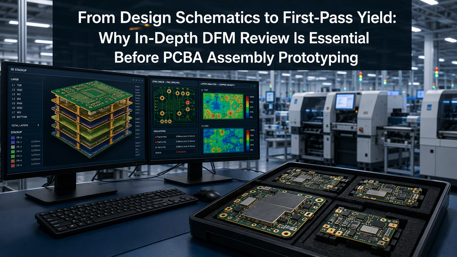
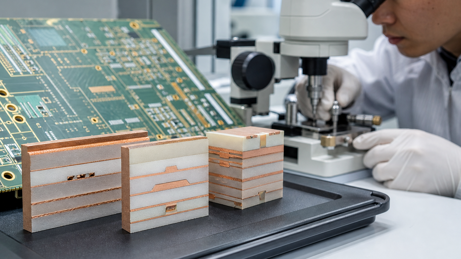 7. PCB Stack-Up Is an Electrical Design Decision
For high-speed PCBAs, the layer stack-up is much more than a manufacturing specification.
It directly affects:
- Impedance
- Signal return paths
- Crosstalk
- Power distribution
- EMI behavior
A multilayer PCB may include:
Signal Layer → Ground Plane → Signal Layer → Power Plane → Signal Layer
The distance between signal traces and reference planes is particularly important.
A smaller dielectric distance can change the required trace geometry for a target impedance.
Therefore, engineers should establish the stack-up early rather than designing the routing first and selecting the stack-up afterward.
8. The Reference Plane Is Part of the High-Speed Signal Path
A high-speed signal does not travel alone.
Its return current also needs a low-impedance path.
For many PCB structures, the return current flows primarily along the reference plane beneath or near the signal trace.
If the signal crosses:
- A split plane
- A large void
- An inappropriate layer transition
the return path may become disrupted.
This can increase loop area and potentially increase:
- EMI
- Crosstalk
- Signal distortion
Therefore, high-speed routing should always consider both the forward signal path and the return-current path.
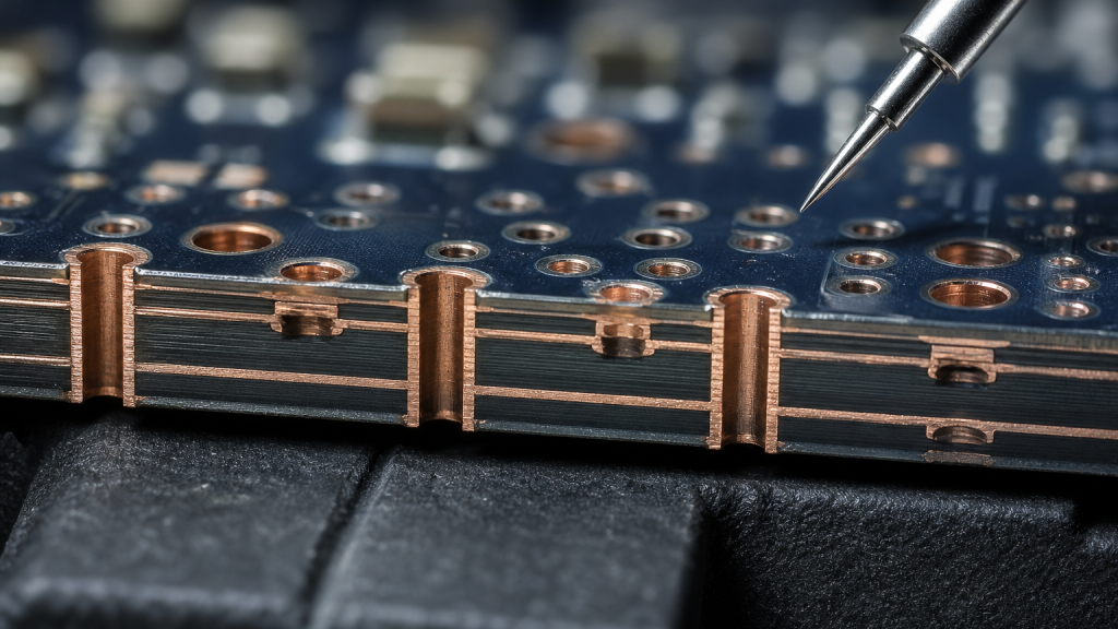
9. Vias Can Create High-Speed Discontinuities
Vias are essential for multilayer PCB routing.
However, at high speeds, a via is not electrically invisible.
A layer transition can introduce:
- Parasitic capacitance
- Parasitic inductance
- Impedance discontinuity
Unused portions of a through-hole via can also create a via stub.
At sufficiently high frequencies, long via stubs can contribute to signal reflection and resonance.
Possible solutions include:
- Back drilling
- Blind vias
- Buried vias
- Optimized via structures
The appropriate solution depends on data rate, stack-up, manufacturing capability, and cost requirements.
 10. Crosstalk: When One Signal Interferes With Another
High-density PCBAs often place many signal traces close together.
When electrical energy from one trace couples into a neighboring trace, crosstalk can occur.
Two common categories are:
- Near-end crosstalk
- Far-end crosstalk
Crosstalk can become more significant when traces are:
- Too close
- Routed in parallel for long distances
- Operating with fast signal transitions
PCB designers can reduce unwanted coupling through:
- Increasing spacing
- Reducing parallel routing
- Using appropriate ground references
- Optimizing layer structures
- Controlling trace geometry
In high-speed PCB design, physical distance can become an electrical design parameter.
11. Connectors Can Become the Weakest Link
A PCB may have carefully controlled impedance, but the signal still has to pass through connectors.
Connectors introduce their own electrical characteristics.
Potential issues include:
- Impedance discontinuity
- Parasitic capacitance
- Parasitic inductance
- Contact variation
- Mechanical tolerances
This means high-speed design cannot stop at the PCB edge.
Engineers need to consider the complete channel:
IC → PCB → Via → Connector → Cable → Connector → PCB → IC
The weakest part of this channel can determine the final signal quality.
12. Signal Integrity Should Be Considered Before PCBA Production
High-speed signal problems are expensive to discover after manufacturing.
Once a PCB has been fabricated and assembled, fixing a fundamental routing problem may require a new PCB revision.
This can increase:
- Prototype costs
- Development time
- Engineering workload
- Product launch risk
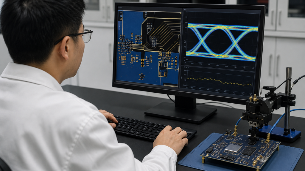
Therefore, Signal Integrity (SI) analysis can be performed before PCB fabrication.
Engineers may simulate:
- Eye diagrams
- Insertion loss
- Return loss
- Crosstalk
- Reflection
- Timing margin
Simulation does not eliminate the need for physical testing.
Instead, it helps identify potential design weaknesses earlier.
13. PCB Material Can Affect High-Speed Performance
FR-4 is widely used in PCB manufacturing, but not all FR-4 materials have identical electrical characteristics.
For high-speed applications, engineers may need to evaluate:
- Dielectric constant
- Dissipation factor
- Dk stability
- Df stability
- Thermal characteristics
For more demanding applications, specialized high-frequency materials may be considered.
Material selection should therefore be based on the actual signal requirements rather than simply choosing a material based on price.
The correct PCB material helps establish a more predictable electrical environment.
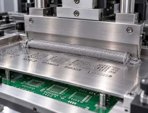
14. PCBA Manufacturing Can Influence High-Speed Performance
High-speed signal integrity is not determined entirely by the PCB design.
The assembly process can also affect electrical behavior.
Relevant factors may include:
- Component placement accuracy
- Solder joint consistency
- Connector installation
- PCB warpage
- Component package variation
For example, high-speed connectors require accurate mechanical positioning.
A manufacturing process that introduces excessive variation can affect the physical signal channel.
This is why high-speed PCB design and PCBA manufacturing should be treated as one engineering system.
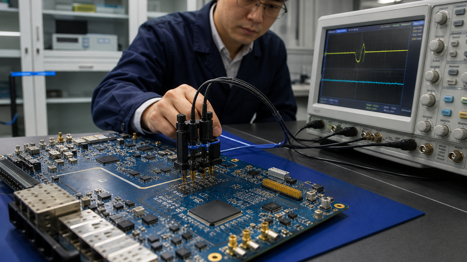
15. Testing a High-Speed PCBA Requires the Right Tools
Traditional multimeter measurements are not enough for many high-speed interfaces.
Engineers may use:
- High-bandwidth oscilloscopes
- Differential probes
- Vector Network Analyzers
- Time-Domain Reflectometry
- Logic analyzers
These tools can help evaluate:
- Eye opening
- Rise time
- Fall time
- Jitter
- Reflection
- Insertion loss
- Return loss
The testing method should match the speed and complexity of the interface.
A measurement system that is too slow can hide the very problem engineers are trying to observe.
16. High-Speed PCBA Is a System-Level Engineering Challenge
One of the biggest lessons from high-speed electronics is that no single design rule guarantees success.
A reliable high-speed PCBA requires coordination between:
- Circuit Design
- PCB Stack-Up
- Signal Routing
- Power Integrity
- Mechanical Design
- PCB Fabrication
- PCBA Assembly
- Electrical Validation
A change in one area can influence another.
For example, moving a connector may require PCB rerouting.
Rerouting may change the reference plane.
Changing the reference plane may alter impedance.
Changing impedance may affect signal integrity.
This interconnected behavior is why high-speed PCBA development requires system-level thinking.
17. The Future of PCB Design Is Moving Toward Channel-Based Engineering
As data rates continue to increase, PCB engineers are gradually moving away from thinking only in terms of individual traces.
Instead, the entire signal channel becomes the object of analysis.
A channel may include:
Transmitter → Package → Via → PCB Trace → Connector → Cable → Connector → PCB Trace → Receiver
Each section contributes to total signal loss and distortion.
This approach allows engineers to identify the true bottleneck rather than optimizing one PCB trace in isolation.
The future of high-speed PCBA design will increasingly combine:
- 3D electromagnetic simulation
- Signal integrity analysis
- Power integrity analysis
- Thermal analysis
- Manufacturing data
This creates a more comprehensive digital engineering workflow.
When Electronics Get Faster, PCB Design Becomes Part of the Circuit
High-speed electronics have changed the role of the PCB.
It is no longer simply a mechanical platform that connects components.
The PCB itself has become an active part of the electrical system.
Its:
- Trace geometry
- Layer stack-up
- Copper structure
- Vias
- Reference planes
- Connectors
- Materials
can all influence the final signal.
For modern PCBA development, reliable high-speed performance depends on controlling the entire electrical channel rather than solving problems one trace at a time.
The most successful high-speed PCB designs therefore begin with a different question.
Not:
“Can we connect these components?”
But:
“Can we control the complete signal path from transmitter to receiver?”
As data rates continue to rise, this mindset will become increasingly important.
The future of PCBA is not simply about placing more components onto smaller boards.
It is about creating a carefully engineered electrical environment where every signal can travel faster, cleaner, and more reliably.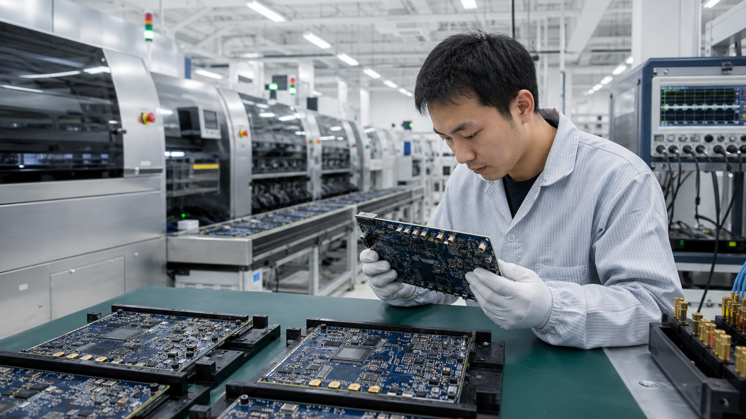


Leave A Comment