
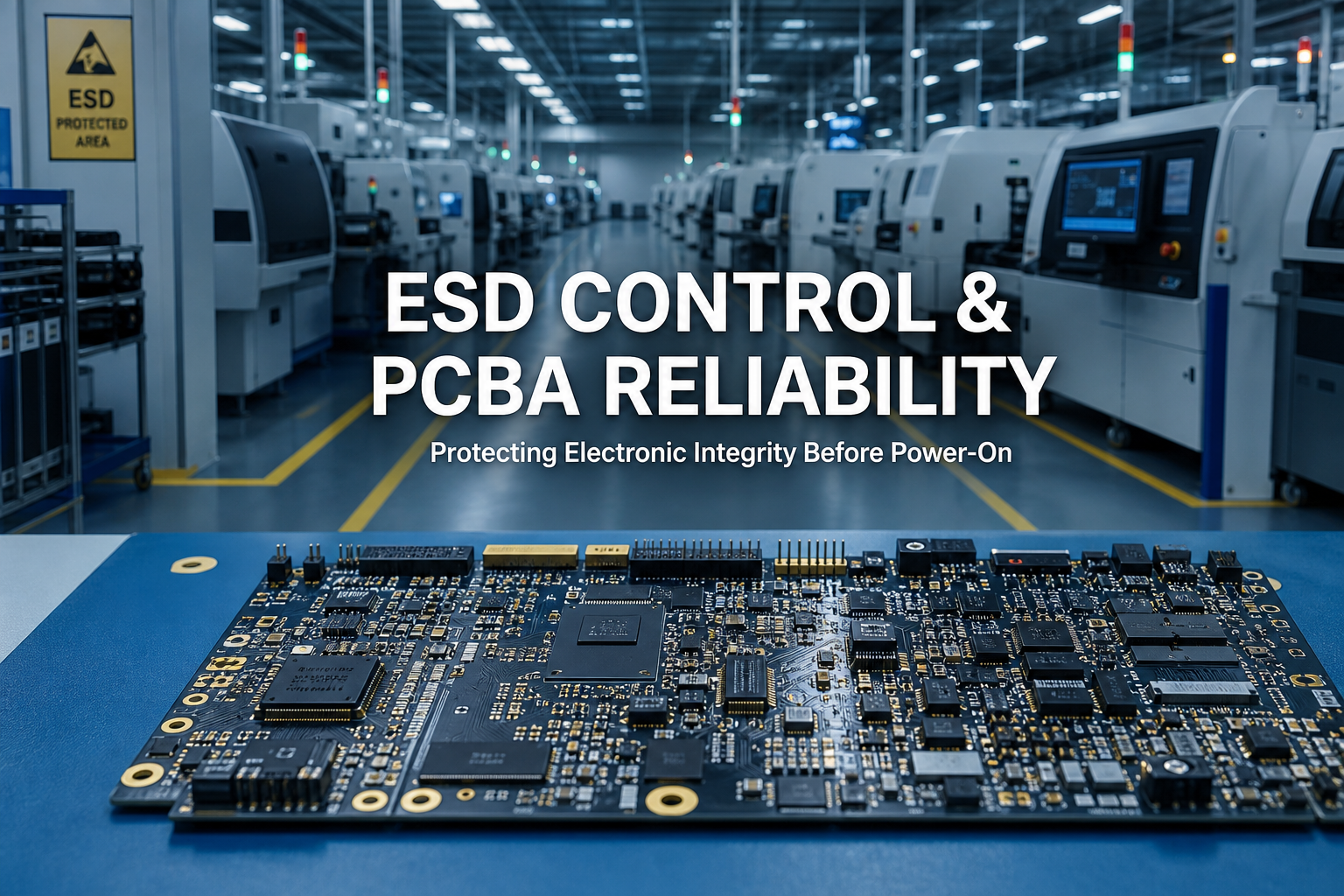
The Damage You Cannot See: How ESD Control Determines PCBA Reliability Before the Product Even Powers On
A Tiny Discharge, a Major Manufacturing Risk
In modern electronics manufacturing, components are becoming smaller, circuits are becoming more sensitive, and operating voltages are continuing to decrease. These developments have improved electronic performance while creating a less visible challenge for PCB assembly manufacturers: electrostatic discharge, commonly known as ESD.
A person walking across a factory floor, a plastic tray moving along a production line, or an operator handling a semiconductor device can generate electrostatic charges. When these charges suddenly transfer between objects with different electrical potentials, an electrostatic discharge may occur.
The discharge can be too small to feel or see, yet powerful enough to damage sensitive electronic components.
Unlike obvious mechanical damage or incorrect component placement, ESD-related failures are not always immediately detectable. A component may pass initial inspection, complete SMT assembly, and even function during early testing, only to develop intermittent faults or premature failure after delivery.
For PCBA manufacturers, ESD protection is therefore not simply a matter of installing anti-static flooring or requiring employees to wear wrist straps. It is a systematic manufacturing discipline that connects component handling, workstation design, equipment grounding, material selection, process monitoring, and quality verification.
Understanding how ESD affects PCBA reliability—and how to control it throughout production—is essential for building dependable electronic products.
 1. What Actually Happens During Electrostatic Discharge?
Electrostatic discharge occurs when accumulated electrical charges move rapidly between objects with different electrical potentials.
In electronics manufacturing, this can happen through several common mechanisms:
- Human body charging: Operators accumulate static electricity through walking, clothing friction, or contact with insulating materials.
- Device charging: Electronic components become electrically charged during handling, transportation, or packaging.
- Field-induced charging: An electrostatic field causes charge redistribution within a nearby conductive object.
- Material separation: Plastic films, packaging materials, conveyor belts, and other insulating surfaces generate electrostatic charges through contact and separation.
The key concern is not simply the voltage generated. The actual damage depends on multiple factors, including discharge current, energy, duration, device sensitivity, and the electrical path through the component.
Two major ESD models are particularly relevant to electronic manufacturing.
Human Body Model (HBM)
The Human Body Model simulates an electrostatic discharge from a charged human body into an electronic device.
It is important because operators frequently handle exposed components during incoming inspection, material preparation, rework, and manual assembly.
Charged Device Model (CDM)
The Charged Device Model describes a situation in which an electronic component itself becomes charged and then rapidly discharges when it contacts a grounded conductor.
CDM events can have extremely fast rise times. This makes them particularly challenging for modern semiconductor devices with small geometries and sensitive internal structures.
An ESD protection strategy must consider both models rather than assuming that controlling human body voltage alone is sufficient.
 2. Why Modern PCBA Components Are More Vulnerable to ESD
The increasing complexity of electronic components has made ESD control more important than ever.
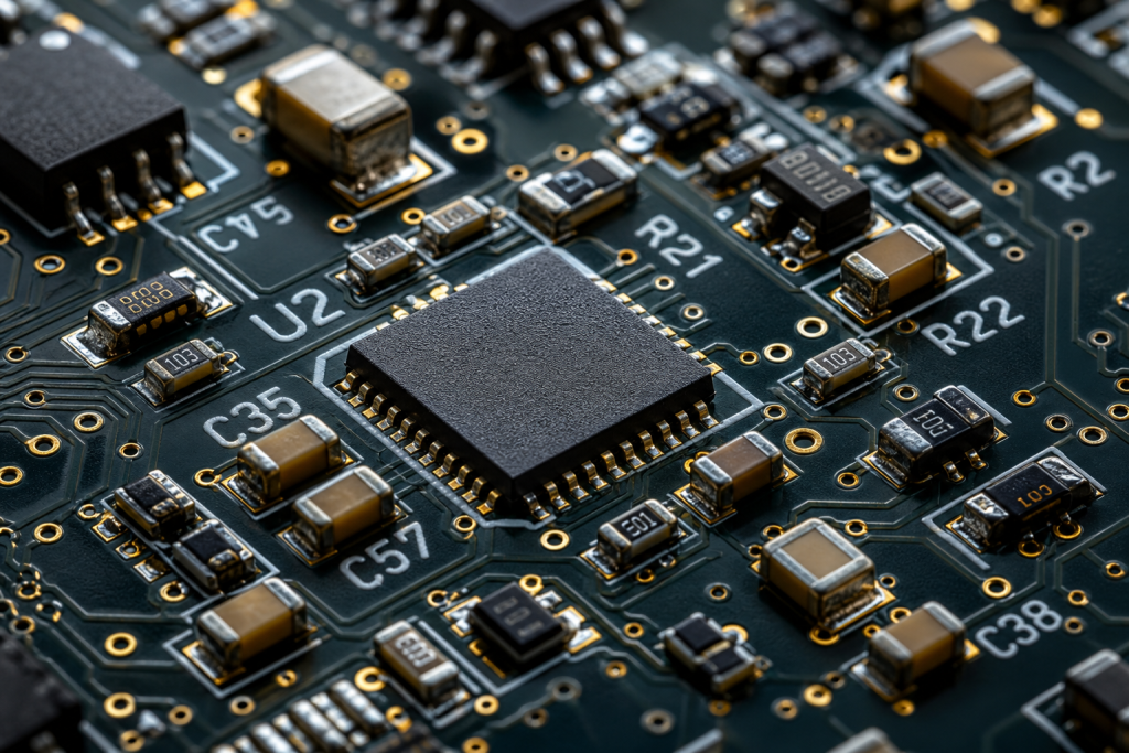
Modern integrated circuits contain extremely small semiconductor structures. As transistor dimensions decrease, internal insulating layers and junction structures may become more sensitive to electrical overstress.
Several component categories deserve particular attention.
Microcontrollers and Application Processors
Microcontrollers, CPUs, and application processors contain complex internal circuits with numerous input/output pins. Damage to an internal protection structure may affect only one functional block, making the defect difficult to identify during basic inspection.
MOSFETs and Power Management Devices
MOSFET gate structures are particularly sensitive to excessive voltage. An ESD event can damage the gate oxide, resulting in increased leakage current, abnormal switching behavior, or complete device failure.
High-Speed Communication ICs
USB, Ethernet, HDMI, RF, and other communication interfaces often incorporate sensitive input structures. ESD damage may cause signal instability, reduced communication performance, or intermittent connectivity.
Sensors and Analog Components
Precision sensors, operational amplifiers, and analog-to-digital converters may experience changes in leakage current, offset voltage, or measurement accuracy following an ESD event.
Not every ESD-damaged component fails immediately. Some devices experience latent damage, in which electrical characteristics deteriorate without producing an obvious initial failure.
This is one reason why ESD prevention must begin before components enter the assembly process.
 3. Where ESD Risks Exist Along the PCBA Manufacturing Process
ESD exposure is not limited to the SMT placement stage. It can occur throughout the entire manufacturing workflow.
3.1 Incoming Material Inspection
Components arrive in packaging designed to provide varying levels of electrostatic protection.
If protective bags are opened in an uncontrolled environment, or if components are transferred into ordinary plastic containers, the original protection may be compromised.
A reliable incoming inspection process should include:
- Verification of ESD protective packaging.
- Inspection of packaging condition and labeling.
- Controlled unpacking procedures.
- Transfer into approved conductive or dissipative storage containers.
- Proper grounding of inspection workstations.
The goal is to preserve the component’s protection from the moment it enters the facility.
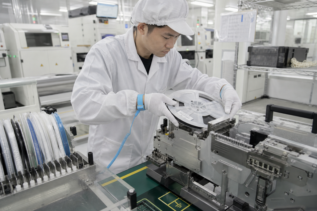
3.2 SMT Material Preparation and Feeder Loading
During SMT preparation, operators handle reels, trays, component tapes, and feeder assemblies.
Although automated placement equipment can reduce direct human contact, material preparation still creates potential ESD exposure.
For example, removing a component reel from an unprotected surface and placing it on an ordinary plastic workbench may introduce an unnecessary charging risk.
Manufacturers should establish ESD-safe material preparation areas, use approved storage materials, and ensure that operators follow controlled handling procedures.
3.3 SMT Assembly and Machine Interfaces
Automated SMT equipment introduces another layer of ESD considerations.
Conveyor systems, feeder mechanisms, component contact surfaces, and equipment maintenance activities can all influence electrostatic conditions.
Manufacturers should evaluate grounding continuity, equipment bonding, conveyor materials, and the suitability of contact surfaces.
It is also important to recognize that an SMT machine being connected to a power supply does not automatically mean that every relevant conductive component is properly grounded.
Grounding must be verified, not assumed.
3.4 Manual Assembly, Inspection, and Rework
Manual operations often involve direct contact with exposed electronic assemblies.
Examples include:
- Through-hole component insertion.
- Connector installation.
- Manual soldering.
- BGA rework.
- Component replacement.
- Electrical inspection and troubleshooting.
These processes require particular attention because operators may handle unprotected PCB assemblies while working with soldering tools, fixtures, and test equipment.
Proper wrist straps, grounded work surfaces, ESD-safe tools, and regular compliance checks are essential.
3.5 Functional Testing and Final Packaging
A PCBA may pass through several production stages before reaching final testing.
During ICT, FCT, firmware programming, and manual debugging, the board may be connected to test fixtures, cables, and external equipment.
If the test setup contains improperly grounded conductive surfaces, the board may become exposed to ESD.
Final packaging is equally important. A properly manufactured PCBA can still be damaged during transportation if it is packed in ordinary non-protective materials.
ESD protection must therefore continue until the product is safely enclosed in suitable packaging.
4. Building an Effective ESD Protected Area (EPA)
An ESD Protected Area, or EPA, is a controlled environment in which electrostatic charge generation and discharge risks are managed.
A properly designed EPA combines people, equipment, materials, and procedures.
4.1 Grounding and Equipotential Bonding
Grounding is one of the foundations of ESD control.
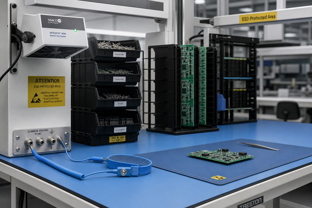
Conductive and dissipative surfaces within the protected area should be connected to an appropriate common grounding system.
This includes:
- ESD workbenches.
- Groundable floor systems.
- Wrist strap connection points.
- Equipment frames.
- Approved grounding accessories.
Equipotential bonding helps prevent dangerous voltage differences between nearby conductive objects.
However, grounding alone is not enough. Insulating materials can retain electrostatic charges even when surrounding equipment is properly grounded.
4.2 Personnel Grounding
Operators should use appropriate personnel grounding systems when handling exposed ESD-sensitive devices.
Common measures include:
- Wrist straps connected to verified grounding points.
- ESD footwear.
- ESD garments.
- Heel grounders or other approved personnel grounding systems.
Wrist straps should be tested regularly, and personnel grounding procedures should be integrated into daily production routines.
4.3 ESD-Safe Work Surfaces and Flooring
Workbenches and flooring should use materials with suitable electrical resistance and charge-dissipation characteristics.
The objective is to prevent rapid charge accumulation while allowing electrostatic charges to dissipate in a controlled manner.
It is important to distinguish between conductive and dissipative materials. Conductive materials provide a relatively low-resistance path, while dissipative materials release charge more gradually.
Selecting the correct material depends on the application, grounding design, and applicable ESD requirements.
4.4 Air Ionization
Some insulating materials cannot be grounded directly.
Examples include plastic component carriers, certain machine covers, and packaging films.
In these situations, ionizers can help neutralize electrostatic charges by generating positive and negative ions.
Ionization is especially useful in areas where sensitive devices are exposed near insulating materials.
However, ionizers require regular performance verification and maintenance. Their effectiveness should not be assumed simply because the equipment is installed.
5. Choosing the Right ESD Packaging and Material Handling Methods
Packaging is an important part of ESD protection because components and PCB assemblies may be moved between departments, production lines, warehouses, and external locations.
Different packaging materials provide different levels of protection.
Static-Dissipative Materials
These materials allow electrostatic charges to dissipate gradually and are commonly used for work surfaces, trays, and component handling containers.
Conductive Materials
Conductive containers and bags provide a relatively low-resistance path for charge movement. They are useful in controlled handling environments.
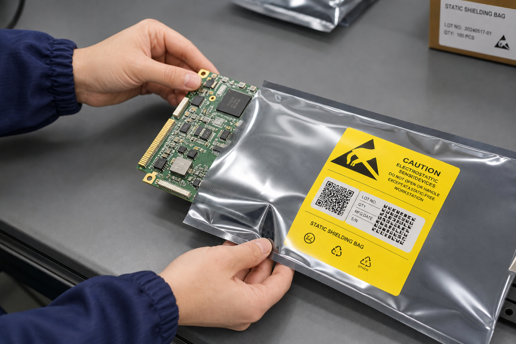
Static-Shielding Bags
Static-shielding bags are designed to protect sensitive electronic components from external electrostatic fields and discharge events.
They are commonly used for transporting individual components, PCB assemblies, and sensitive electronic modules.
ESD-Safe Trays and Reels
Approved trays and reels help maintain protection during material storage and transportation.
Manufacturers should avoid replacing approved ESD packaging with ordinary plastic containers simply because they are more convenient or less expensive.
A consistent packaging standard helps reduce unnecessary handling risks and improves production traceability.
 6. ESD Monitoring: How Do Manufacturers Know the Protection Is Working?
An ESD control program should be supported by measurable verification rather than relying entirely on employee awareness.
Several monitoring methods can be incorporated into routine production management.
Wrist Strap Testing
Wrist straps should be tested using suitable testers to verify that the grounding connection and resistance remain within the required limits.
Testing frequency should be defined by the facility’s ESD control program and relevant standards.
Surface Resistance Testing
ESD work surfaces, flooring, and other materials can be evaluated using appropriate resistance measurement instruments.
These tests help determine whether materials continue to meet their specified electrical properties.
Grounding Verification
Grounding points, equipment bonding, and connections should be inspected and measured periodically.
Loose connections, damaged cables, or incorrect installation can reduce the effectiveness of an otherwise well-designed system.
Field and Charge Measurements
Electrostatic field meters and charge measurement equipment can help identify areas where charge accumulation occurs.
Ionizer performance should also be verified through suitable testing methods.
ESD Audit Records
Manufacturers should maintain records of:
- Personnel grounding test results.
- Workstation inspection results.
- Grounding system verification.
- Ionizer performance checks.
- Training records.
- Corrective actions.
- Periodic ESD audits.
These records help identify recurring problems and provide evidence that ESD controls are being maintained.
7. Connecting ESD Control with PCBA Quality Management
ESD management should not operate as an isolated factory safety activity. It should be connected directly to the broader PCBA quality management system.
For example, when an electrical test identifies abnormal leakage current, unexpected component behavior, or intermittent communication failures, ESD damage may be one possible cause.
However, these symptoms can also result from incorrect component selection, soldering defects, circuit design problems, or other manufacturing issues.
A structured failure analysis process is therefore necessary.
Combining ESD Records with Production Traceability
A modern manufacturing system can connect ESD inspection records with production information, including:
- PCB serial numbers.
- Component lot numbers.
- SMT production batches.
- Workstation identification.
- Operator and shift information.
- Inspection results.
- ICT and FCT test records.
- Rework history.
If a potential ESD-related issue is discovered, these records can help narrow down the affected production window and identify possible exposure points.
Using Electrical Testing to Identify Potential Damage
Different tests can reveal different types of component abnormalities.
- ICT: Helps identify electrical connectivity issues, component value deviations, and certain short/open conditions.
- FCT: Verifies actual board functionality under defined operating conditions.
- Leakage current testing: Can help identify abnormal electrical behavior in relevant circuits.
- Communication testing: Evaluates interface stability and signal transmission.
- Burn-in testing: Can expose certain early-life failures under controlled operating conditions.
It is important to understand that no single test can guarantee the detection of every ESD-damaged component.
A component with latent damage may pass initial testing and fail only after prolonged operation or exposure to specific environmental conditions.
This makes prevention more effective than depending entirely on final inspection.
8. Standards That Support a Professional ESD Control Program
A structured ESD management system should be based on recognized industry standards and appropriate technical requirements.
Several important references include:
ANSI/ESD S20.20
This standard establishes requirements for developing, implementing, and maintaining an ESD control program. It provides a framework for controlling electrostatic discharge in environments that handle sensitive electronic items.
IEC 61340-5-1
This international standard addresses the protection of electronic devices from electrostatic phenomena. It provides requirements and guidance for establishing an ESD control program.
ANSI/ESD S541
This standard addresses packaging materials for ESD-sensitive items and helps manufacturers select appropriate packaging solutions.
IEC 61340 Series
The broader IEC 61340 family includes standards and test methods covering electrostatic phenomena, materials, measurement, and control.
Manufacturers should identify the applicable standard versions and customer-specific requirements when establishing their ESD procedures.
Compliance should be supported by documented processes, verification activities, training, and continuous improvement—not simply by purchasing anti-static equipment.
9. Why ESD Control Matters to Customers Choosing a PCBA Manufacturing Partner
When selecting a PCBA supplier, buyers often evaluate production capacity, SMT equipment, component sourcing, inspection capabilities, and delivery performance.
These factors are important, but they do not tell the entire story.
A manufacturer may operate advanced SMT machines and sophisticated inspection equipment, yet still face reliability risks if its ESD management is inadequate.
For customers, several questions can help evaluate a supplier’s ESD capabilities:
- Does the factory have clearly defined ESD protected areas?
- Are personnel grounding systems tested and documented?
- Are ESD-safe materials used during component handling and PCB assembly?
- Are production equipment and workstations included in grounding verification?
- Are ESD audits performed regularly?
- Can the manufacturer trace production batches and investigate potential ESD-related failures?
- Are ESD requirements included in employee training and quality procedures?
A professional PCBA partner should be able to explain how ESD controls are implemented across incoming inspection, SMT assembly, manual operations, testing, and packaging.
The objective is not merely to prevent visible failures. It is to reduce the possibility of hidden electrical damage that may affect product performance after shipment.
10. From ESD Prevention to Long-Term PCBA Reliability
As electronic products continue to become smaller, faster, and more functionally integrated, ESD protection will remain a fundamental requirement in electronics manufacturing.
The challenge is that electrostatic damage often occurs without visible evidence. A component can look perfect, a solder joint can pass visual inspection, and a PCBA can power on normally—yet its internal electrical characteristics may already have been affected.
This is why effective ESD management must be built into the manufacturing process rather than treated as an additional inspection step.
A reliable strategy combines controlled handling, personnel grounding, suitable materials, equipment verification, ESD-safe packaging, production traceability, and continuous employee training.
For PCB assembly manufacturers, this approach supports more than defect reduction. It helps protect component performance, improve manufacturing consistency, reduce unexpected failures, and strengthen customer confidence.
Ultimately, PCBA reliability is determined by much more than how accurately components are placed or how well solder joints are formed. It also depends on controlling the invisible electrical risks that exist throughout the manufacturing journey.
The best ESD protection is the damage that never happens.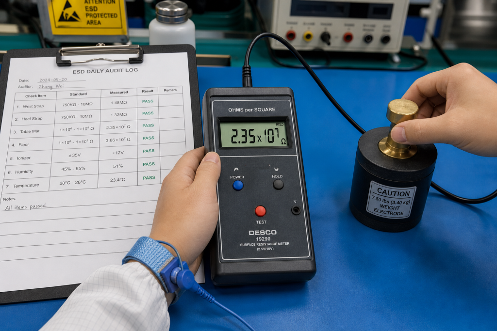










Leave A Comment