

High-Precision PCB SMT Manufacturing Synergy and Quality Control in Turnkey PCBA Mode
In modern electronic hardware development, circuit board integration continues to increase, and fine-pitch components are widely applied. To overcome supply chain fragmentation and communication overhead in traditional outsourced manufacturing, more innovative enterprises prefer turnkey services. Integrating bare PCB fabrication, BOM procurement, precision SMT assembly, and electrical testing into a unified workflow helps eliminate manufacturing risks through early engineering reviews. This article provides an in-depth analysis of how high-precision PCB SMT manufacturing and turnkey PCBA models achieve efficient synergy and quality control.
1. Why Does High-Precision SMT Placement Rely Heavily on Upstream Material and Bare Board Control?
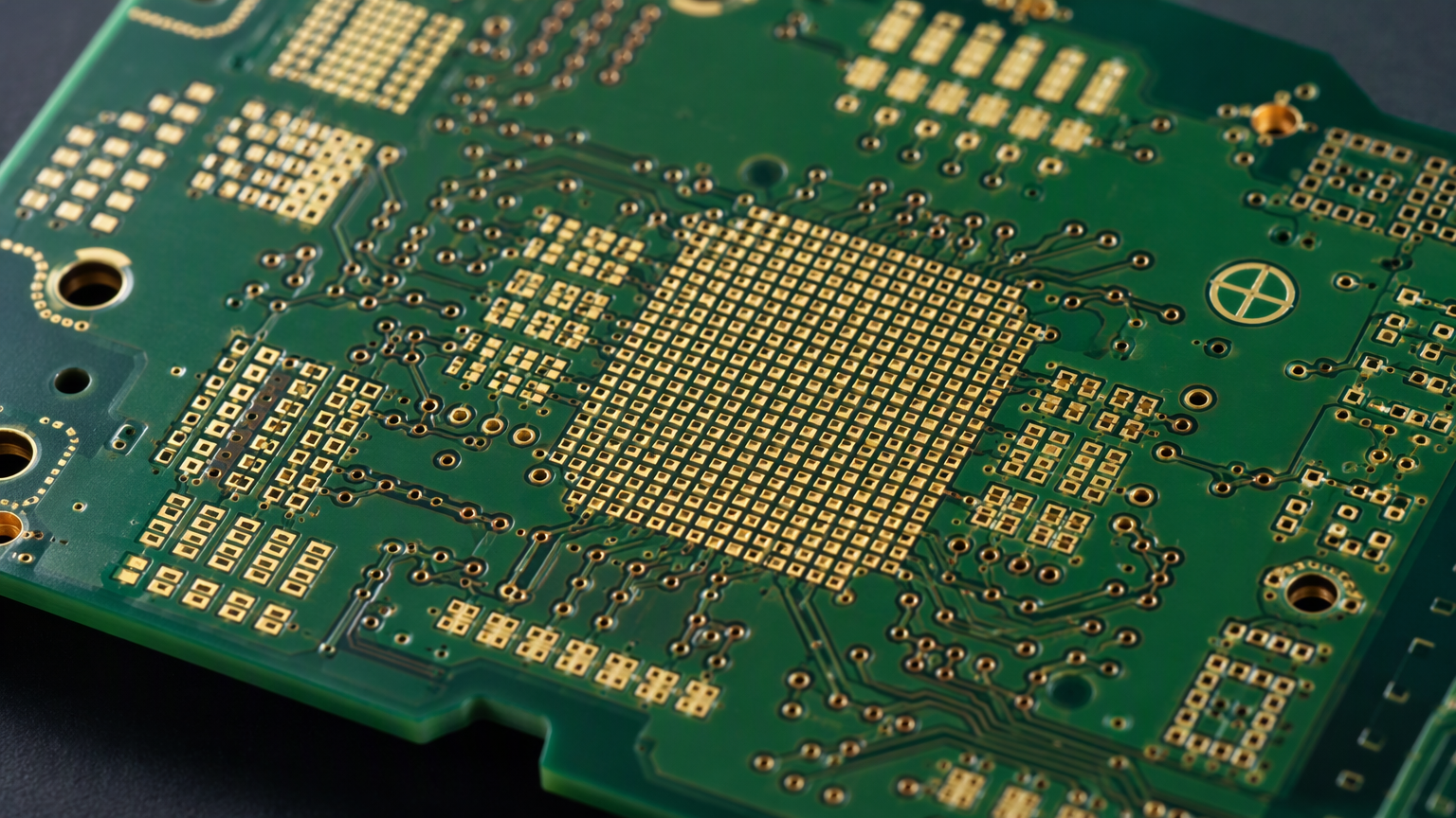
1.1 Bare Board Flatness and Surface Finish Determine Printing Quality
Fine-pitch packages have strict requirements for bare PCB flatness. If the circuit board exhibits slight warpage, solder paste printing thickness will deviate. Chemical gold (ENIG) and OSP surface finishes provide excellent coplanarity. Compared with traditional hot air solder leveling, they provide uniform contact surfaces for micro pads. This helps prevent solder paste bridging and solder ball defects.
Under the turnkey PCBA model, the engineering team directly controls bare PCB tolerances. Engineers verify solder mask bridge thickness and alignment accuracy before tooling. Meanwhile, the manufacturing team optimizes panelization borders based on assembly requirements. This upfront synergy ensures the stability of high-precision PCB SMT printing from the source.
1.2 Component Packaging and Solderability Impact Placement Accuracy
High-speed SMT pick-and-place machines are sensitive to component tape packaging. Loose parts or damaged carrier tapes easily cause component throwing and feeder jams. Once component leads oxidize, reflow soldering produces cold solder joints and voids. These issues reduce production throughput and increase rework costs.
Qualified turnkey services maintain strict incoming quality control (IQC). The warehouse performs humidity monitoring and baking for moisture-sensitive devices (MSD). Meanwhile, engineers verify carrier tape dimensions and nozzle compatibility. Systematic material management ensures continuous and stable SMT equipment operation.
2. In-Depth DFM and BOM Engineering Review: Eliminating Assembly Risks Before Production
2.1 Automated Cross-Verification of BOM and CAD Coordinate Data
File auditing is a critical pre-production step. The engineering team verifies the customer’s BOM against Gerber photoplotter files. Meanwhile, technicians import Centroid pick-and-place coordinate data. The system automatically cross-checks component footprints, pad dimensions, and pin polarities.
This rigorous verification identifies design conflicts early. For example, reversed silkscreen markings or mismatched footprint sizes can be corrected before production. By resolving data ambiguities, the production team avoids line stoppages and material waste.
2.2 Stencil Aperture Design and Component Density Balance
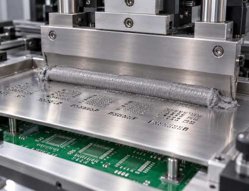
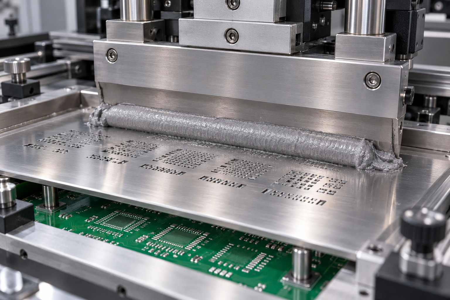
Complex circuit boards often combine micro components with large connectors. A single-thickness laser stencil struggles to satisfy solder volume requirements for both. Excess solder paste causes shorts on fine-pitch leads. Insufficient paste causes insufficient wetting on power components.
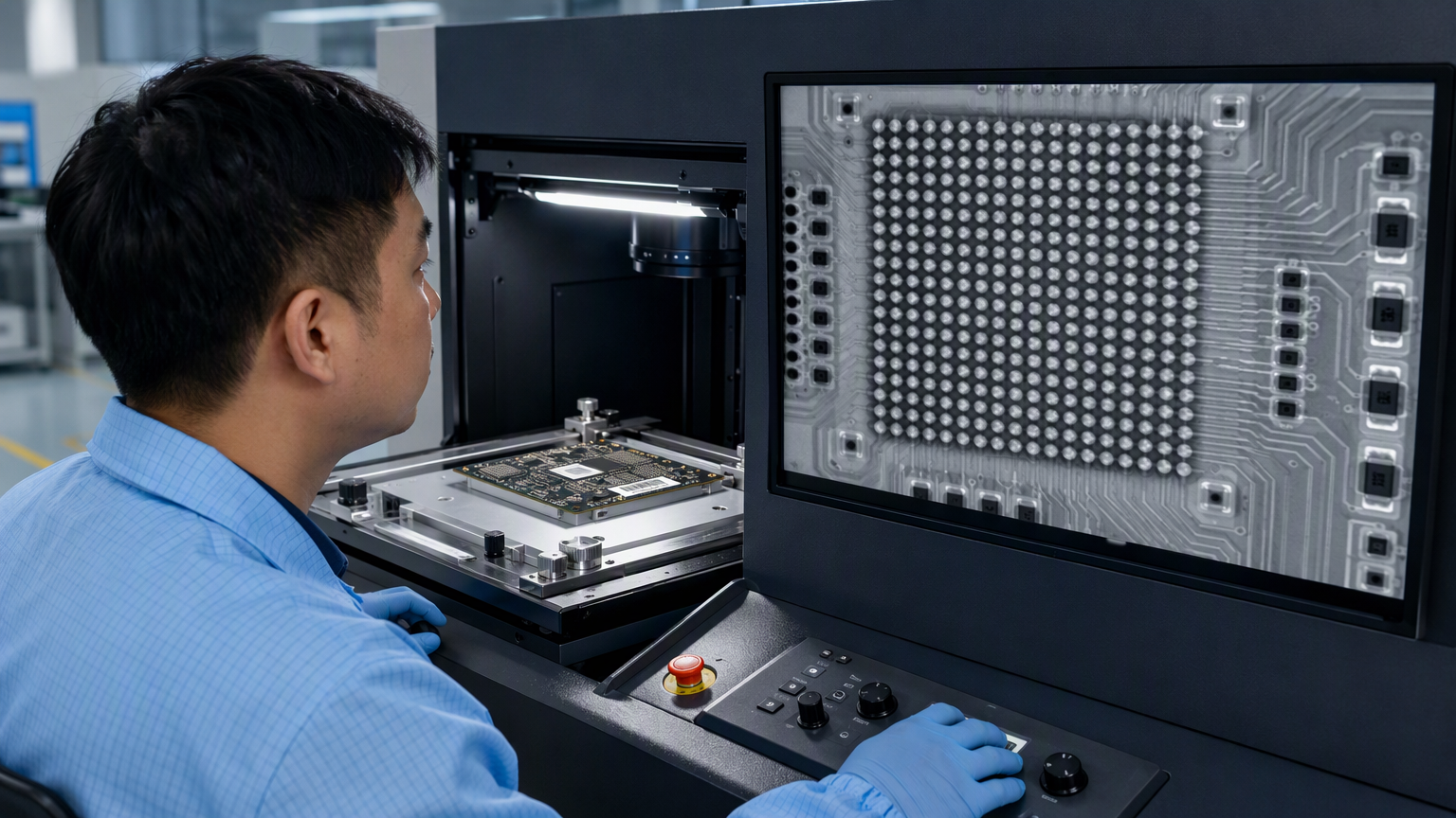
Through Design for Manufacturability (DFM) analysis, engineers can design step stencils. Apertures are thinned locally for dense leads and thickened for large solder pads. Meanwhile, sufficient optical fiducial marks are placed on panel margins. A proper layout significantly improves the alignment accuracy of SMT optical cameras.
3. Core Processes and Parameter Control in High-Precision SMT Assembly
3.1 3D SPI Solder Paste Inspection: Intercepting Printing Defects Before Placement
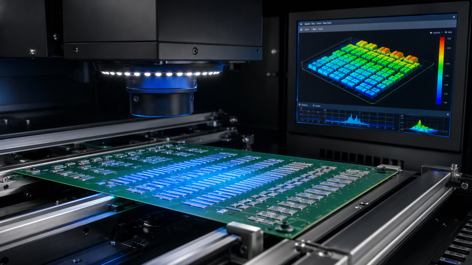
Solder paste printing is a critical stage in the surface mount process. Most soldering defects originate from abnormal solder paste volume or geometry. Deploying an inline 3D SPI system before the pick-and-place machine enables comprehensive pad measurement. The inspection system quantifies solder paste height, area, and volume distribution.
When insufficient paste, bridging, or alignment offsets occur, the system triggers an alert. Defective boards are diverted before component placement. Operators can wash and reprint the board immediately. This real-time interception prevents expensive ICs from being soldered onto defective boards.
3.2 Placement Accuracy and Multi-Zone Reflow Soldering Profile Optimization
High-precision SMT mounters are equipped with high-resolution flying vision cameras. Robotic arms automatically correct component centers and rotation angles during high-speed movement. Micro leads land precisely on target pads. This establishes a solid foundation for high-reliability solder joints.
The subsequent reflow soldering process requires scientific thermal parameter configuration. The technical team uses temperature profiling boards to capture actual thermal zone data. By optimizing ramp-up rates, soak times, and peak temperatures, solder paste melts completely within the process window. Precise temperature control minimizes tombstoning and solder spatter.
4. Comprehensive Inspection System: Building a Quality Loop for Hidden Solder Joints
4.1 3D AOI Optical Inspection: Accurately Identifying Surface Assembly Conditions
After reflow soldering, the PCBA moves directly to the 3D AOI inspection station. The optical system scans the board surface using multi-angle structured light. Algorithms reconstruct three-dimensional models of solder joints and components. The system automatically identifies missing parts, wrong components, polarity reversals, and poor wetting angles.
Compared with manual visual inspection, automated optical inspection provides greater objectivity. Inspection accuracy is not compromised by operator visual fatigue. Detection data is logged into the quality system to support ongoing SMT parameter optimization.
4.2 High-Resolution X-Ray and Electrical Testing: Inspecting Bottom-Terminated Packages
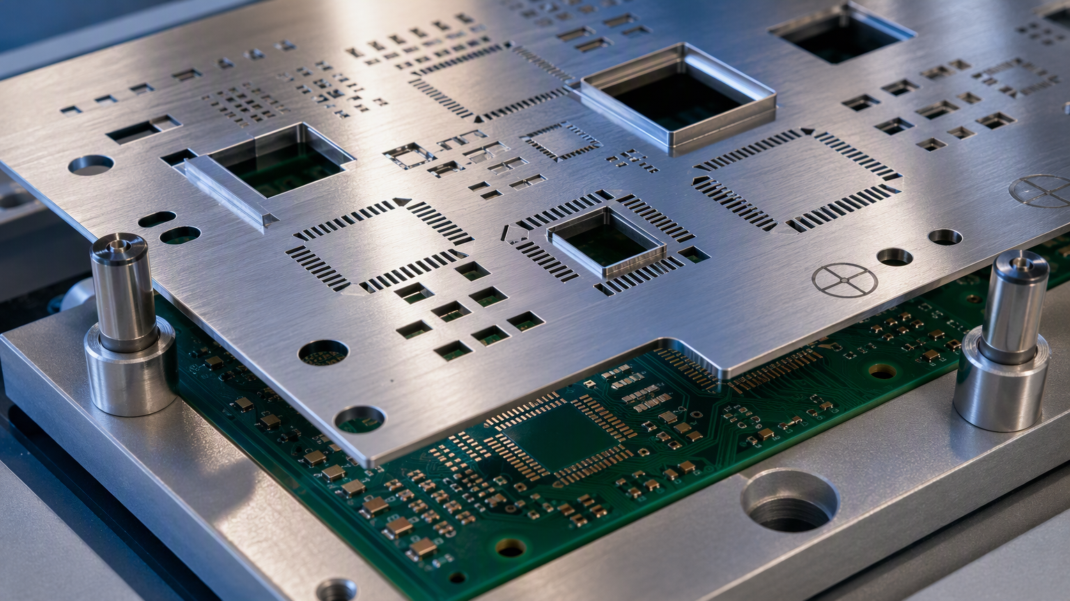
For complex ICs using BGA, QFN, and LGA packages, optical lenses cannot inspect bottom solder joints. Industrial high-resolution X-Ray inspection systems are required. X-Ray penetration reveals internal solder ball structures clearly. Engineers can evaluate solder wetting, bridging, and voiding percentages directly.
After visual and optical verification, products undergo electrical testing. Technicians build flying probe or functional testing (FCT) fixtures according to project specifications. By applying rated voltages and test signals, the team verifies full circuit performance. A strict test loop guarantees functional integrity upon final delivery.
5. Supply Chain Transparency and Material Traceability in Turnkey PCBA Mode
5.1 Authorized Component Sourcing Channels and Counterfeit Prevention
Material authenticity is the foundation of electronic manufacturing quality. Reliable turnkey PCBA suppliers source directly from original manufacturers or authorized tier-one distributors. Every batch of electronic components includes formal certificates of conformity and lot documentation. This procurement standard prevents refurbished or counterfeit components from entering production lines.
For high-value or scarce ICs, incoming inspection includes lead solderability testing. Rigorous supply chain management protects intellectual property and hardware assets. A transparent bill of materials gives hardware engineering teams complete confidence.
5.2 Full-Process Lot Tracking and Electrostatic Discharge Protection
The production workshop must maintain an effective electrostatic discharge (ESD) grounding network. Operators, workstations, and equipment operate within certified ESD safety thresholds. Sensitive components are stored in temperature- and humidity-controlled dry cabinets. These environmental controls prevent potential electrostatic breakdown.
Concurrently, the manufacturing plant implements barcode tracking systems. Each PCB is assigned a unique serial identifier. Component lot numbers, SMT machine records, reflow profiles, and quality inspection reports are linked to the board ID. Comprehensive records provide reliable data support for maintenance and quality traceability.
6. Cost-Efficiency and Risk Boundaries: From Prototyping to Volume Delivery
6.1 Evaluating Hidden Management Costs and Development Cycle Compression
Hardware teams sometimes overlook the hidden overhead of fragmented material logistics. Independent purchasing consumes procurement resources and generates separate shipping costs. Material shortages or staggered delivery times repeatedly delay SMT production schedules.
Selecting a turnkey PCBA model significantly shortens the hardware development cycle. Customers communicate through a single engineering interface for materials and manufacturing coordination. Engineering teams can focus resources on core firmware and hardware feature development. Overall project efficiency improves substantially.
6.2 Defining Clear Engineering Ownership and Engineering Change Management
In traditional fragmented outsourcing, product faults often lead to responsibility disputes. Assembly plants may question bare board quality, while board fabricators question component solderability. The turnkey PCBA model consolidates manufacturing accountability under a single service provider.
When designs iterate, the Engineering Change Notice (ECN) workflow responds promptly. The system freezes obsolete materials and updates pick-and-place programs and stencils simultaneously. Unified change control prevents batch scrap caused by revision mismatches.
7. How to Scientifically Evaluate and Select a Turnkey PCBA Manufacturing Partner?
7.1 Multi-Dimensional Evaluation: Engineering Capability, Inspection Equipment, and First-Article Prototyping
When evaluating suppliers, procurement teams should prioritize engineering responsiveness. Professional engineering teams provide thorough DFM reports prior to production. Key indicators include placement accuracy, inline SPI and AOI coverage, and X-Ray inspection capabilities. High-reliability projects also require verification of functional testing procedures.
If you are looking for a reliable turnkey manufacturing partner, prepare your complete engineering package. When you choose our PCBA services, our engineering team will evaluate design feasibility and clarify cost boundaries. Submit your Gerber files, BOM with complete manufacturer part numbers, pick-and-place coordinate data, and functional test specifications. Our engineers will provide detailed process recommendations and high-precision PCB SMT assembly solutions based on your project data.
Conclusion: Building Core Competitive Advantages Through Manufacturing Synergy
The integration of high-precision SMT assembly and turnkey PCBA models represents the direction of modern electronics manufacturing. It is more than turnkey component procurement; it is end-to-end engineering synergy from design to delivery. By implementing strict material control and DFM reviews, the manufacturing team resolves process risks prior to production.
In downstream operations, advanced SMT placement equipment and comprehensive inspection systems safeguard solder joint quality. Partnering with a professional turnkey PCBA manufacturer reduces management overhead and accelerates reliable hardware delivery. Applying rigorous manufacturing standards ensures that innovative hardware succeeds in competitive global markets.










Leave A Comment